BoundaryBox
Chip boundary square with corner crosses (legacy BoundBox, layer 9/0 → qcc chip_boundary).
Source: Quantcore. Category: marker. Module: quantcore_circuits.layouts.others.markers.
See also the catalog.
Pins
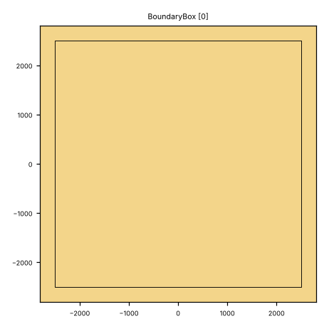
Pin image (default parameters). Light = metal, dark = etched gap, colours = junction layers. A red dot and arrow is a pin and its direction (out of the cell); the red bar is the CPW width a + 2 b. Blue dot = a pin without direction. Units: µm.
No pins: this cell has no ports. Place it with at= / rot=.
Parameters
name |
default |
unit |
description |
|---|---|---|---|
|
|
μm |
Width of center conductor |
|
|
μm |
Width of gap |
|
|
μm |
Turn radius |
|
|
μm |
Box size |
|
|
μm |
Corner cross half-length |
|
|
– |
Layer (qcc or KQC name) |
Electrically relevant parameters (sizes, gaps, junction, ports) come first, the rest follows.
LOM model
none (a LOM build gives each pin its own bare node, without elements).
How to use
In Python:
from quantcore_circuits.designer import Designer

d = Designer("demo", box=(0, 0, 7500, 7500))
d.add("U1", "BoundaryBox", at=(3750, 3750), a=10)   # parameters: see the table above
# no directed pin: place it with at= / rot=, or snap it with snap= / to=
Pin names go into d.route(...) as INSTANCE.pin, and into snap= / to= when placing. From the shell: qcc components BoundaryBox lists the pins; add --schema for the parameters.
In KLayout: Quantcore panel ▸ Components ▸ double-click the cell, then click on the layout to place it. Rotate and mirror before the click; use Connect on two pins to route.
GUI status (kplugin/COMPONENTS_STATUS.md): places ok, edit ok, connect n/a (no directed port), build ok. chip-frame box (5010 um).