Demo chip (KQC)
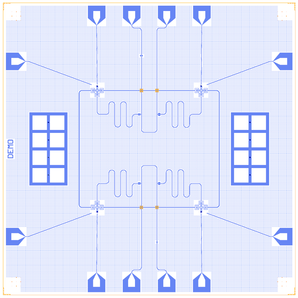
KQCircuits’ demonstration chip: four flux-tunable Swissmon qubits in a ring, read out through two probe lines, each with its own charge line and flux line. It is the standard KQC example, rebuilt on the Quantcore PDK (sapphire, Quantcore die frame, Quantcore trilayer junctions).
Build it to see a complete multi-qubit chip made from KQC components: ARD24 launchers, readout capacitors and T’s, meandered resonators, ring couplers and control lines.
At a glance
Notebook |
|
Source |
KQCircuits |
Chip |
10 × 10 mm, ARD24 sample-holder launchers |
On the chip |
4 Swissmons · 4 λ/2 readouts (5000 to 5300 µm) · 2 probe lines · 4 ring couplers · 4 charge and 4 flux lines · 2 junction-test arrays |
Builds today |
yes (layout built on 2026-11-19 in 12 s) |
How the notebook builds it
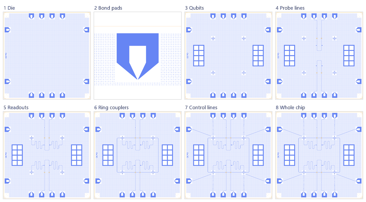
Die. The empty 10 × 10 mm chip with the Quantcore frame (dicing marks, alignment grids, chip boundary, device ID) and the ARD24 launchers.
Bond pads. The launchers moved so their outer etch edge sits 100 µm from the die edge (the pad rule).
Qubits. Four Swissmons at KQC’s positions with Quantcore SQUIDs.
Probe lines. Readout capacitors and T’s, then the two probe lines.
Readouts. Four λ/2 meandered resonators from the qubits to the capacitors.
Ring. Four couplers join neighbouring qubits into a ring.
Control lines. Charge and flux lines from the launchers.
Whole chip. Sim groups, content centred in the die, design saved.
LOM estimates
Numbers are from a run of this notebook on 2026-11-19 (Setup, Design, Check and the LOM cells, 18 s): QuCat normal modes with QuTiP dressed values.
group |
qubit |
f_q (GHz) |
α (MHz) |
resonator |
f_r (GHz) |
κ (MHz) |
χ (MHz) |
|---|---|---|---|---|---|---|---|
QB1+RR1 |
QB1 |
5.81 |
-200 |
RR1 |
11.38 |
2.9 |
-0.115 |
QB2+RR2 |
QB2 |
5.81 |
-200 |
RR2 |
11.07 |
11.8 |
-0.118 |
QB3+RR3 |
QB3 |
5.81 |
-200 |
RR3 |
10.96 |
4.23 |
-0.121 |
QB4+RR4 |
QB4 |
5.81 |
-200 |
RR4 |
10.72 |
8.12 |
-0.125 |
group |
pair |
ZZ (kHz) |
neighbours |
hybridised |
|---|---|---|---|---|
ring |
QB1-QB2 |
– |
yes |
yes |
ring |
QB2-QB3 |
– |
no |
yes |
ring |
QB2-QB4 |
– |
yes |
yes |
ring |
QB1-QB3 |
– |
yes |
yes |
ring |
QB1-QB4 |
– |
no |
yes |
ring |
QB3-QB4 |
– |
yes |
yes |
pair |
f₋ (GHz) |
f₊ (GHz) |
g = Δf/2 (MHz) |
|---|---|---|---|
QB1+QB2 |
6.002 |
6.008 |
2.84 |
QB2+QB4 |
6.002 |
6.008 |
2.84 |
QB4+QB3 |
6.002 |
6.008 |
2.84 |
QB3+QB1 |
6.002 |
6.008 |
2.84 |
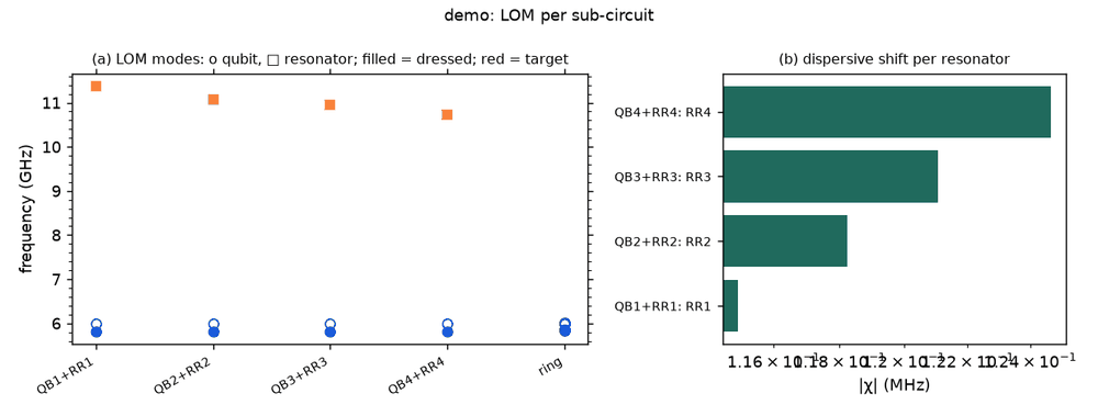
These are lumped-model estimates (component formulas and calibration), not FEM results; see the LOM page for how far to trust them.
Build spec
The rest of this page is the detailed spec the notebook was built from: every component, port, route and length.
Source other-libs/KQCircuits-main/KQCircuits-main/klayout_package/python/kqcircuits/chips/demo.py (Demo) ·
GPL-3.0 (IQM Finland). The notebook rebuilds the chip from extracted parameters and uses KQC cells through the registry; no KQC code is
copied. What it is: 4 flux-tunable Swissmons in a ring of 4 CPW buses. Each qubit has a meandered readout
resonator, coupled through a finger capacitor and a T to one of 2 probelines, plus a drive line and a flux line. There
are 2 junction-test arrays. 10 × 10 mm. The KQC frame is already (0,0)–(10000,10000), so no shift is needed.
Face 1t1, KQC default layers. Checked on 2026-11-02 with plan_design: every route length
below equals the KQC build to 0.01 µm, and d.lom() connects everything (no unconnected ports).
Coordinates were read from a scratch build of the KQC chip, which gives the refpoints. Default chip parameters
(a=10, b=6, r=100) apply unless a value is given.
Components
instance |
catalog ref |
key params (units) |
at (x, y) |
rot |
notes |
|---|---|---|---|---|---|
QB1 |
|
|
(3220, 7000) |
0, |
cplr0 W (3001,7000), cplr1 S (3220,6781), cplr2 E (3439,7000), drive (3020,7200), flux N (3220,7245.33) |
QB2 |
|
same |
(6780, 7000) |
180 |
cplr0 E, cplr1 S (6780,6781), cplr2 W, drive (6980,7200) |
QB3 |
|
same |
(3220, 3000) |
0 |
cplr1 N (3220,3219), drive (3020,2800), flux S (3220,2754.67) |
QB4 |
|
same |
(6780, 3000) |
180, |
cplr1 N (6780,3219), drive (6980,2800) |
C1–C4 |
|
|
(4656.5,6181) / (5343.5,6181) / (4656.5,3819) / (5343.5,3819) |
0 / 180 / 0 / 180 |
readout coupling C; port a faces the resonator |
PL1–PL4 |
|
|
(4734,6181) / (5266,6181) / (4734,3819) / (5266,3819) |
270 / 90 / 270 / 90 |
snap |
CIN1 |
|
|
(4734, 8192) |
270 |
series input capacitor of probeline 1 |
CIN2 |
|
|
(5266, 1808) |
90 |
series input capacitor of probeline 2 |
testarray_w/e |
|
|
(900,3750) / (7800,3750) |
0 |
no ports |
Routes
route |
from → to |
type, length (µm) |
waypoints |
notes |
|---|---|---|---|---|
CPL12 |
QB1.cplr2 → QB2.cplr2 |
cpw a=4 b=9, 3122.0 |
(3839,7000), wp(6161,7000, n_bridges=3) |
bus |
CPL24 |
QB2.cplr0 → QB4.cplr0 |
cpw a=4 b=9, 4714.16 |
(7399,7000), wp(7399,3000, n_bridges=3) |
bus |
CPL43 |
QB4.cplr2 → QB3.cplr2 |
cpw a=4 b=9, 3122.0 |
(6161,3000), wp(3839,3000, n_bridges=3) |
bus |
CPL31 |
QB3.cplr0 → QB1.cplr0 |
cpw a=4 b=9, 4714.16 |
(2601,3000), wp(2601,7000, n_bridges=3) |
bus |
DLk |
chip.DL-QBk → QBk.drive |
cpw 2478.23, |
QB1 (780,8000), QB2 (9220,8000), QB3 (780,2000), QB4 (9220,2000) |
diagonal straight into the directionless drive port |
FLk |
chip.FL-QBk → QBk.flux |
cpw 2074.77 |
wp((QBk.x, 7345.333 or 2654.667), n_bridges=4) |
20 µm jog in x, slanted |
RR1 |
QB1.cplr1 → C1.a |
meander=5000 |
(3220,6181), (3520,6181), (4520,6181) |
meander auto-placed on (3520→4520) |
RR2 |
QB2.cplr1 → C2.a |
meander=5100 |
(6780,6181), (6480,6181), (5480,6181) |
|
RR3 |
QB3.cplr1 → C3.a |
meander=5200 |
(3220,3819), (3520,3819), (4520,3819) |
|
RR4 |
QB4.cplr1 → C4.a |
meander=5300 |
(6780,3819), (6480,3819), (5480,3819) |
|
PL1_in / PL1_a / PL1_b / PL1_out |
chip.PL-1-IN → CIN1.a / CIN1.b → PL1.left / PL1.right → PL2.left / chip.PL-1-OUT → PL2.right |
1344.66 / 1968.5 / 1646.16 / 3376.16 |
[(4400,9220),(4734,9220)] / [wp(4734,7000, airbridge)] / [(4734,5570), wp(5266,5570, n_bridges=1)] / [(5600,9220),(5266,9220), wp(5266,7000, airbridge)] |
airbridges where the probeline crosses CPL12 |
PL2_in / PL2_a / PL2_b / PL2_out |
chip.PL-2-IN → CIN2.a / CIN2.b → PL4.left / PL4.right → PL3.left / chip.PL-2-OUT → PL3.right |
same lengths |
[(5600,780),(5266,780)] / [wp(5266,3000, airbridge)] / [(5266,4430), wp(4734,4430, n_bridges=1)] / [(4400,780),(4734,780), wp(4734,3000, airbridge)] |
crosses CPL43 |
Verified Designer code (J: the source gives no junction values, so pick them from targets):
L = {2: "FL-QB1", 3: "PL-1-IN", 4: "PL-1-OUT", 5: "FL-QB2", 7: "DL-QB2", 12: "DL-QB4",
     14: "FL-QB4", 15: "PL-2-IN", 16: "PL-2-OUT", 17: "FL-QB3", 19: "DL-QB3", 24: "DL-QB1"}
d = Designer("kqc_demo", launchers={"type": "ARD24", "assign": L}, chip={"name_chip": "Demo"})
SW = dict(cpl_length=[120, 120, 120], port_width=[4, 10, 4]); W = Designer.waypoint
q = {1: d.add("QB1", "Swissmon", at=(3220, 7000), mirror=True, junction=J, **SW),
     2: d.add("QB2", "Swissmon", at=(6780, 7000), rot=180, junction=J, **SW),
     3: d.add("QB3", "Swissmon", at=(3220, 3000), junction=J, **SW),
     4: d.add("QB4", "Swissmon", at=(6780, 3000), rot=180, mirror=True, junction=J, **SW)}
d.route("CPL12", q[1].cplr2, q[2].cplr2, a=4, b=9, nodes=[(3839, 7000), W((6161, 7000), n_bridges=3)])  # + CPL24/43/31
for k, (x, y, rot, nf, xt, xm, Lr) in {1: (4656.5, 6181, 0, 4, 3520, 4520, 5000), 2: (5343.5, 6181, 180, 8, 6480, 5480, 5100),
                                      3: (4656.5, 3819, 0, 5, 3520, 4520, 5200), 4: (5343.5, 3819, 180, 7, 6480, 5480, 5300)}.items():
    c = d.add(f"C{k}", "FingerCapacitorSquare", at=(x, y), rot=rot, finger_number=nf)
    d.add(f"PL{k}", "WaveguideCoplanarSplitter", snap="bottom", to=c.b, lengths=[11, 11, 41], port_names=["right", "left", "bottom"])
    d.route(f"RR{k}", q[k].cplr1, c.a, meander=Lr, nodes=[(3220 if k in (1, 3) else 6780, y), (xt, y), (xm, y)])
d.route("DL1", "chip.DL-QB1", q[1].drive, nodes=[(780, 8000)], term2=6)
d.route("FL1", "chip.FL-QB1", q[1].flux, nodes=[W((3220, 7345.333), n_bridges=4)])          # + DL/FL 2..4
ci = d.add("CIN1", "FingerCapacitorTaper", at=(4734, 8192), rot=270, finger_number=6, taper_length=20)
d.route("PL1_in", "chip.PL-1-IN", ci.a, nodes=[(4400, 9220), (4734, 9220)])
d.route("PL1_a", ci.b, "PL1.left", nodes=[W((4734, 7000), airbridge=True)])               # + PL1_b, PL1_out, PL2_*
Launchers, pads, test structures, markers, labels
ARD24 with KQC names (only the 12 assigned pads are drawn). N: FL-QB1 #2 (3200,9320), PL-1-IN #3 (4400,9320), PL-1-OUT #4 (5600,9320), FL-QB2 #5 (6800,9320). E: DL-QB2 #7 (9320,8000), DL-QB4 #12 (9320,2000). S: FL-QB4 #14 (6800,680), PL-2-IN #15 (5600,680), PL-2-OUT #16 (4400,680), FL-QB3 #17 (3200,680). W: DL-QB3 #19 (680,2000), DL-QB1 #24 (680,8000).
Junction-test arrays W/E (see the table). The chip frame, markers and the “Demo” name come from the DesignChip base.
LOM node structure (qubit ↔ resonator ↔ feedline ↔ bus ↔ control lines)
QBk: island with C to ground and a SQUID to ground; cplr0/1/2 nodes each have C_g and C to ground (Swissmon model: Xmon-scaled estimates).
Bus ring QB1–QB2–QB4–QB3–QB1. Each CPL route is one conductor in the LOM (plain cpw), so for example QB1.cplr2 and QB2.cplr2 merge. In reality the buses are long (3.1/4.7 mm, about λ/2 at 13–19 GHz), so treat them as wires only as a first approximation.
RRk: λ/2 TLres at QBk.cplr1 (meander port↔port). Ck gives the series C to the probeline node.
Probeline 1: chip.PL-1-IN, CIN1, {PL1, PL2}, chip.PL-1-OUT (QB1, QB2). Probeline 2: chip.PL-2-IN, CIN2, {PL4, PL3}, chip.PL-2-OUT (QB4, QB3). Each splitter is one node, and the launchers are 50 Ω ports.
DLk becomes a
drivecontrol on QBk and FLk aflux_biascontrol on J_QBk. Lumped f(RR) ≈ 12.1–12.8 GHz (λ/2, PDK sapphire). KQC sizes the chip for silicon.
Targets (if stated)
None in the source, which is geometry only. readout_res_lengths=[5000,5100,5200,5300], include_couplers=True.
Simplifications for a first rebuild
Skip
testarray_w/eand the airbridgen_bridges. Keep the airbridge waypoints at the four probeline–bus crossings, which would otherwise be galvanic crossings.d.drc()on the full rebuild (tested) gives only twono_lomwarnings, for the test arrays.include_couplers=Falsevariant: drop CPL*. KQC then also drops the probeline airbridges.Quantcore-flow variant (λ/4 + κ in the LOM): drop Ck/PLk/CINk, run each probeline as one cpw route (chip.PL-1-IN → chip.PL-1-OUT via x=4734/5266), and use
RRk → PL.hanger(...)on its vertical segment. Not KQC geometry.
Quantcore PDK rebuild
The notebook is a Quantcore-PDK rebuild of the source chip. The netlist, LOM and imported components are kept, and the process is Quantcore’s.
Notebook: examples/designs/kqc/demo.ipynb.
Chip: the Quantcore die frame (L dicing markers 1000/0, 3 × 3 alignment grids 1001/0, chip boundary 100/0, device ID where an edge is free; any brand text is QCT), drawn on the source’s 10 × 10 mm chip (its launchers sit on the chip edges, so the design does not fit the 7.5 mm die). KQC’s ChipFrame (dicing edge, corner markers, labels) is not drawn. KQC’s original grids its whole ground plane (
with_grid, 5 µm squares on a 10 µm step). The rebuild keeps that coverage at the PDK density instead (chip parametercheese: "chip",with_grid: false): 5 µm squares with 20 µm gaps over the whole die, at least 4 µm from the 3/0 keep-outs, inside the design area and clear of the frame markers and the device ID.Stack: sapphire 650 µm, εr 10.25 (the PDK default stack, used by the LOM estimates and every FEM export); KQC’s own simulation default is silicon (εr 11.45), so LOM capacitances and resonator frequencies here are for sapphire.
Junctions: Quantcore Nb/AlOx/Nb trilayer junctions (
junction_typefromlayouts.registry.trilayer_junction): fingers on 2/0 + 4/0, spacer 50/0 with the 51–53/0 gradient, sized on the PDK junction rule (Nb Δ = 1.4 meV, I_c·R_n = πΔ/2e, R_n·A 13.5 kΩ·µm² and C_J 50 fF/µm² assumed); every Swissmon’s SQUID becomes a PDK SQUID of two 0.25 × 0.6 µm junctions → R_n = 45 kΩ in parallel, L_J = 6.73 nH at zero flux, C_J = 15 fF (in the 40–50 kΩ window). KQC’sjunction_widthsets the straight finger. This replaces the assumed Lj 16 nH + 2 fF. Expected f_q ≈ 5.8 GHz (was 3.94 GHz), still below the ≈ 11–12 GHz λ/2 readouts (estimate from the pre-rebuild LOM C_Σ). The twoJunctionTestPadsarrays get the same Quantcore SQUID.Kept: the topology and every KQC element with the source’s parameters, positions and orientations, the launcher assignment, every route’s path and length, the sim groups (readouts 5000–5300 µm, the ring couplers, the junction-test arrays).