HSQ junction test pads (chip_08)
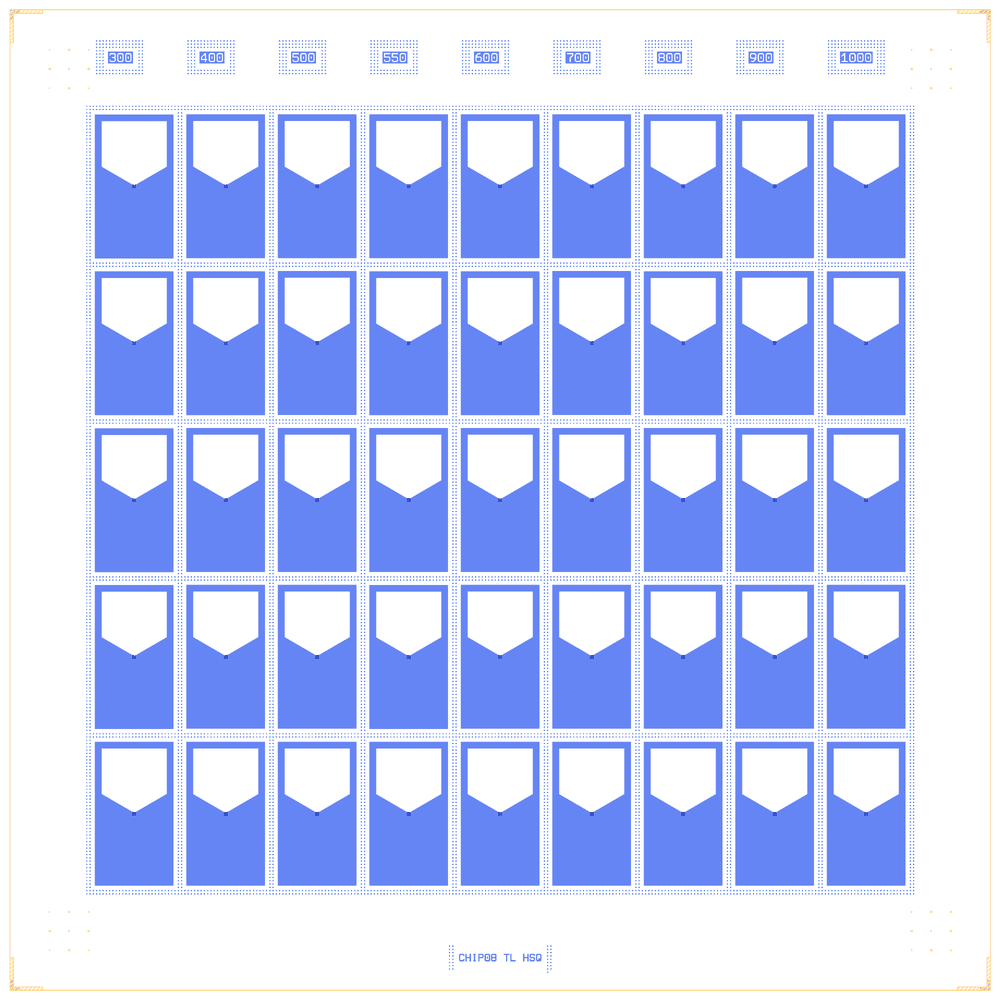
A calibration chip for Josephson junctions. It holds 45 probe structures in a 9 × 5 grid. Each has two large pads whose tips meet in a small window with an HSQ-spacer trilayer junction between them. Measuring the resistance across a pair tells how big that junction really came out. The straight finger is swept from 0.3 to 1.0 µm along the nine columns (labels 300 to 1000, in nm); the bent finger is 0.6 µm in every row. There are no qubits or resonators.
It comes from Quantcore’s QWri script chip_08_TL_HSQ_testpads.py (May 2024, internal). The rebuild adds the PDK die frame (device ID CHIP08 TL HSQ) and the PDK cheese band, and values the junctions on the PDK junction rule without resizing them. Build it to see how a test chip is one cell repeated on a grid with one parameter swept.
At a glance
Notebook |
|
Source |
Quantcore legacy QWri script |
Chip |
7.5 × 7.5 mm Quantcore die, sapphire |
On the chip |
45 |
Builds today |
yes, rebuilt from its JSON on 2026-11-19 in 1.1 s (the notebook itself was not re-run) |
Pictures
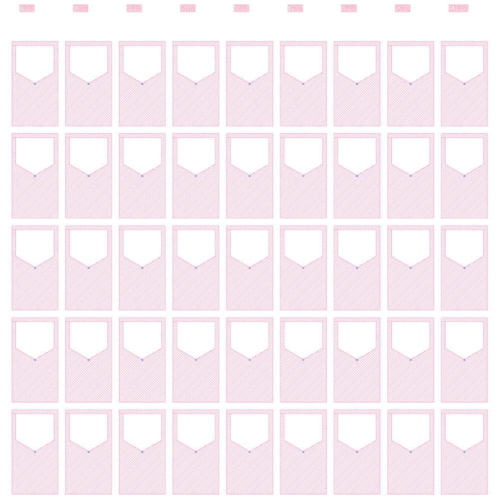
The original legacy layout (render of the legacy GDS).
The rebuild: nine columns of different finger width (300 to 1000 nm), five rows of the same.
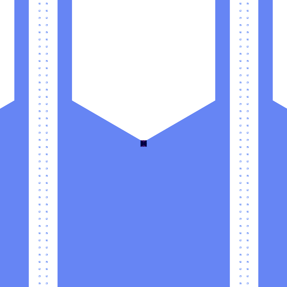
One test pad (the 600 nm column, middle row): two 500 µm pads with the junction at the tip.
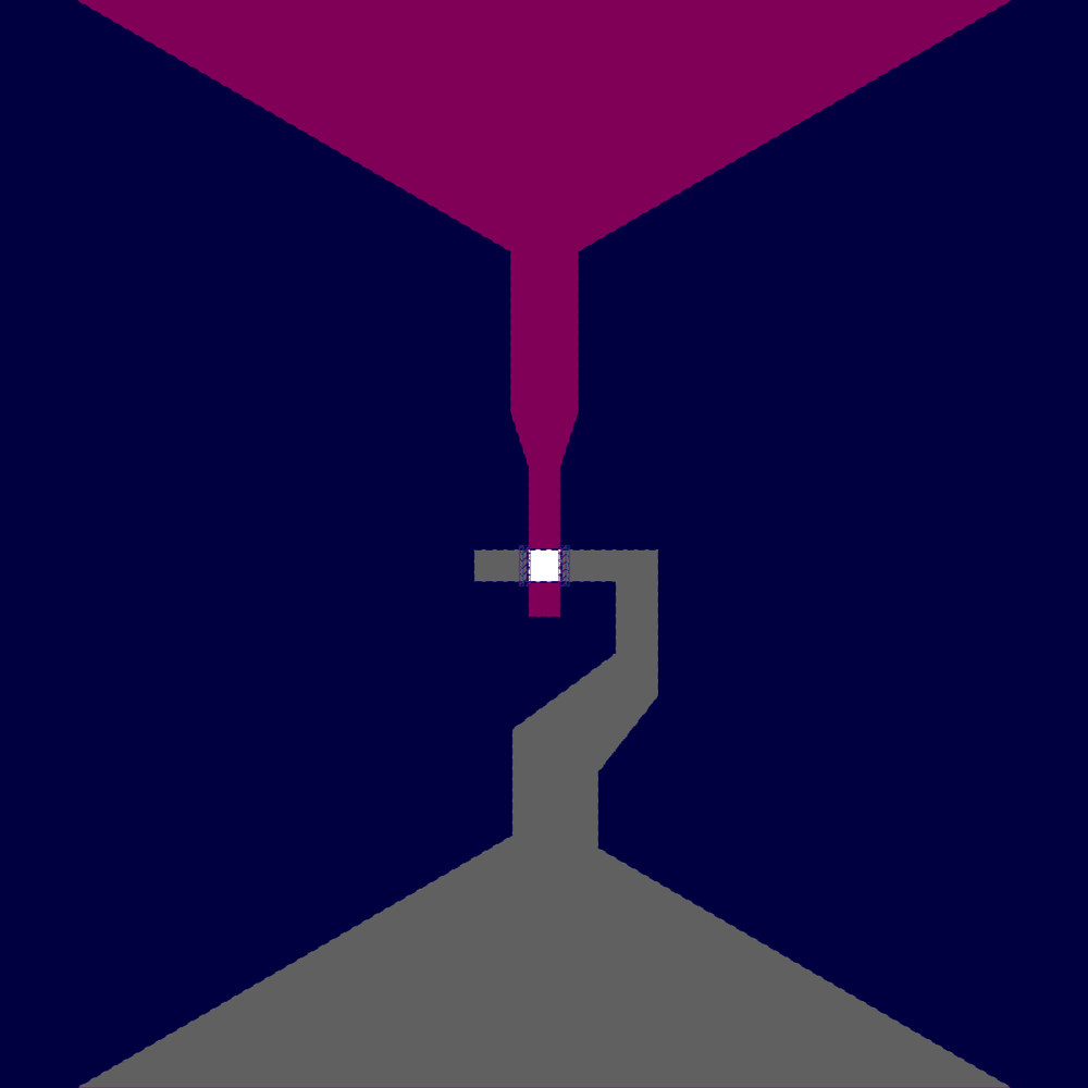
The 20 µm window at the pad tips, where the two fingers overlap to form the junction.
LOM estimates
The notebook has no saved LOM output. The chip has no qubit or resonator, so its LOM netlist is empty.
Build spec
The rest of this page is the detailed spec the notebook was built from: every component, the changes made while rebuilding, and the notes.
Source: components/python/chip_08_TL_HSQ_testpads.py (create_test_chip(), writes
chip_08_TL_HSQ_testJJ_1.0.gds). Legacy QWri library (May 2024), Quantcore internal. Notebook
examples/designs/legacy/chip_08_tl_hsq_testpads.ipynb.
Changes made in the rebuild
Junctions: the drawn test-pad sweep valued on the PDK junction rule (Nb trilayer, Δ = 1.4 meV, I_c·R_n = πΔ/2e = 2.20 mV, R_n 40–50 kΩ, qubits 4–8 GHz; PDK process
get_pdk().junction: R_n·A 13.5 kΩ·µm², C_J 50 fF/µm², both assumed by the PDK).The notebook’s JSON was rebuilt from its layout cell. The notebook has not been re-run, so its outputs are cleared and its PNGs may be out of date.
What it is: a junction-size calibration chip for the HSQ-spacer trilayer process: a 9 × 5 array of
testPad_Nb_TL_HSQ probe structures (chip_04’s grid with chip_06’s HSQ pad) on a 7.5 × 7.5 mm die centred on (0, 0)
→ Designer (x + 3750, y + 3750). The straight (bottom) finger is swept 0.3 … 1.0 µm along the columns; the bent (top)
finger is 0.6 µm in every row. PDK v2 die frame: it replaces the base-metal corner Markers (rot 1/2/3/0; the first
with thickness 50, width 500) and the layer-10 outline with its four 500 µm boxes at (±3350, ±3350). The HSQ corner
markers are kept. No qubits, resonators or feedline. The script also imports junction_creator_HSQ and testPad
but never calls them; its header comment (“50 junctions”, 11 × 5 fingers) is stale: the code draws 9 × 5 = 45.
Builds: yes. Every cell has a catalog ref.
Components (legacy frame)
instance |
legacy cell → catalog ref |
params |
at |
notes |
|---|---|---|---|---|
TP_i_j (45) |
|
pads 500 × 400, middle 300, window 600 × 1100, HSQ boxes (legacy 500/52/53/54 → PDK 50/0 …); straight finger |
x = −2800 … 2800 (700 pitch, |
column i: bf = [0.3, 0.4, 0.5, 0.55, 0.6, 0.7, 0.8, 0.9, 1.0] µm; row j: tf = 0.6 µm ( |
HSQ0 … HSQ3 |
|
|
(−3750, −3750) rot 1, (3750, −3750) rot 2, (3750, 3750) rot 3, (−3750, 3750) rot 0 |
HSQ alignment; the base-metal markers → PDK frame |
LBL_i (9) |
|
|
(x_i − 190, 3350) |
column labels (straight finger in nm); the “BOT” and row labels are commented out in the source |
Designer frame: TP_i_j at (950 + 700 i, 6150 − 1200 j); LBL_i at (760 + 700 i, 7100); the HSQ markers at the die corners.
Routes, test pads, LOM
No routes, no launchers. The test pads and markers have no ports, the labels are port-less shapes: the LOM netlist
is empty. “LOM simulation” = the junction table: area = bf × 0.6 µm², L_J and R_n from
circuit.bridges.lj_from_area / rn_from_area with an assumed Jc (not in the source or the PDK: to be confirmed).
No sim groups, no FEM jobs.
Keep-outs
Legacy positions kept. The outermost windows end at |x| = 3100, |y| = 2950 (legacy), inside the design area and
clear of the corner marker areas; the labels sit at y ≈ 3350 … 3450. The HSQ markers sit at the die corners, in the
dicing-marker areas (DRC frame_margin / frame_keepout, as on chip_05/06). The device ID (CHIP08 TL HSQ) has the
bottom edge centre free.