Nine coupled Xmons (design 12)
A coupled-qubit test chip. A 20/12 µm feedline crosses the die and nine λ/4 readout resonators hang off it, each ending at one of nine Xmon qubits (four above the feedline, five below). The chip tests two things: a direct coupling between two neighbouring qubits (Q1 and Q2, arm tips facing each other) and a tunable coupler, where a flux-tunable qubit (Q8) sits between two others (Q5 and Q6). Each qubit has its own 50 Ω launchpad for a flux line or a drive line.
It comes from Quantcore’s earlier Qiskit Metal design notebook 12.0 Coupled_chip_layout.ipynb (internal). The rebuild keeps every Metal component through the metal: wrapper and moves all launchpads to the 100 µm pad rule, adds the PDK die frame (device ID D12) and cheese band, and swaps the junction footprints for PDK junctions and SQUIDs (45 kΩ). Build it to see a large Metal-style layout with routed flux and drive lines.
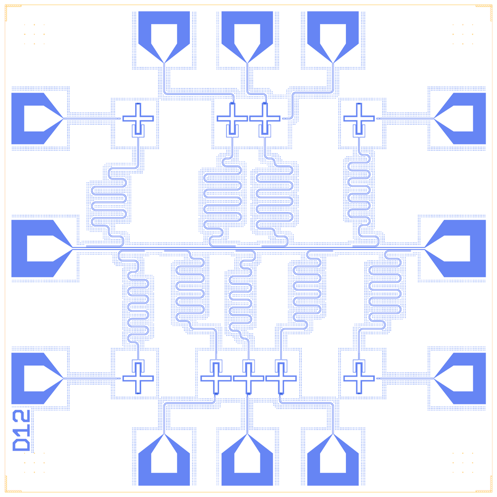
At a glance
Notebook |
|
Source |
Quantcore’s earlier Qiskit Metal notebook |
Chip |
7.5 × 7.5 mm Quantcore die, sapphire, feedline 20 / 12 µm, resonators 10 / 6 µm |
On the chip |
9 |
Builds today |
yes, rebuilt from its JSON on 2026-11-19 in 4.6 s (the notebook itself was not re-run) |
Pictures
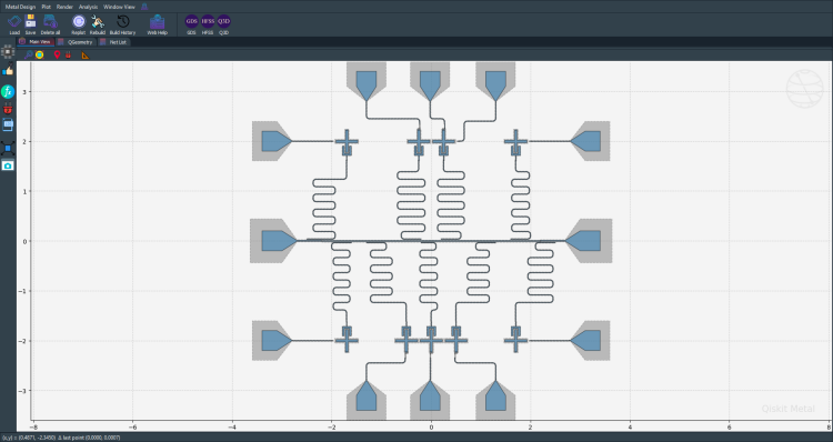
The original design as drawn in the Qiskit Metal GUI (screenshot of the legacy notebook).
The rebuild on the Quantcore PDK, with the die frame and cheese band.
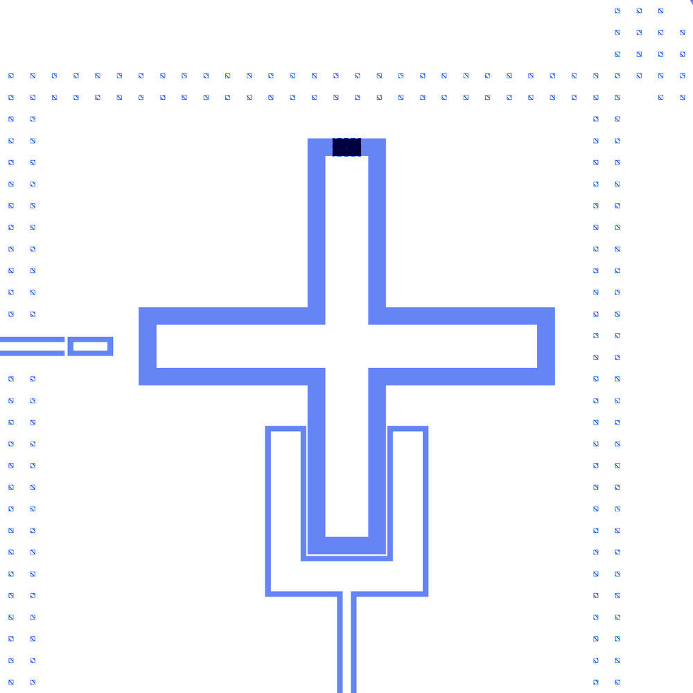
Q0: an Xmon cross with its resonator’s claw below and the junction at the top.
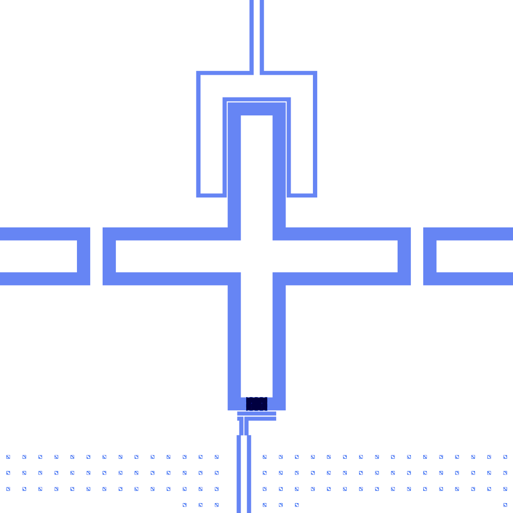
Q8, the tunable coupler: a flux line enters below, and neighbouring qubit arms face it on both sides.
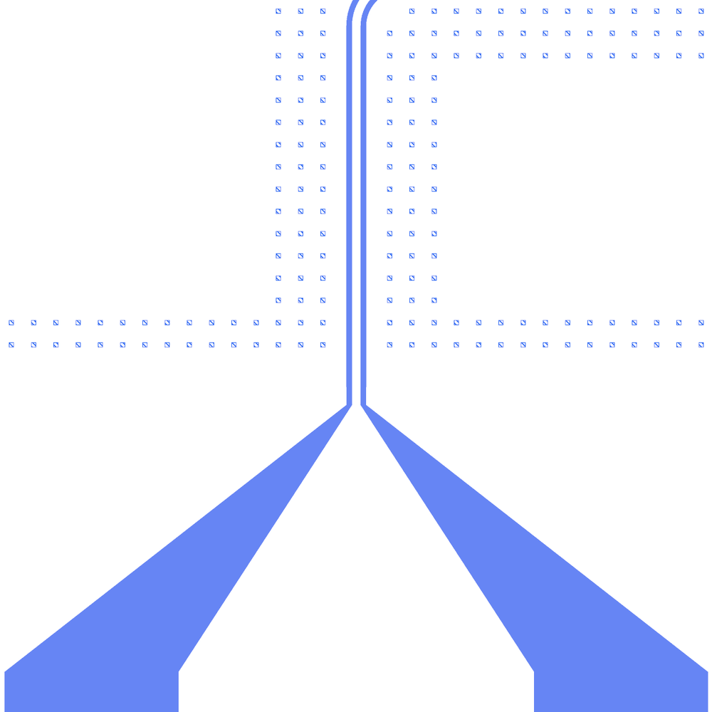
One launchpad: a bond pad tapering into a 20 µm line that is routed to a qubit.
LOM estimates
The notebook’s saved LOM output (QuCat normal modes). Readout frequencies have no targets in this design.
group |
qubit |
f_q (GHz) |
α (MHz) |
resonator |
f_r (GHz) |
κ (MHz) |
χ (MHz) |
|---|---|---|---|---|---|---|---|
Q0+R0 |
Q0 |
5.0591 |
-196.9 |
R0 |
4.9357 |
0.411 |
64.7 |
Q1+R1 |
Q1 |
5.0411 |
-146 |
R1 |
4.4242 |
0.153 |
-1.64 |
Q2+R2 |
Q2 |
5.0401 |
-145.2 |
R2 |
4.5015 |
0.161 |
-2.37 |
Q3+R3 |
Q3 |
5.0325 |
-146 |
R3 |
5.7585 |
0.323 |
-1.59 |
Q4+R4 |
Q4 |
5.0331 |
-146.4 |
R4 |
5.937 |
0.354 |
-1.16 |
Q5+R5 |
Q5 |
5.0248 |
-135.7 |
R5 |
5.226 |
0.165 |
-11 |
Q6+R6 |
Q6 |
5.0277 |
-139.6 |
R6 |
5.283 |
0.216 |
-7.82 |
Q7+R7 |
Q7 |
5.046 |
-124.6 |
R7 |
4.8085 |
0.192 |
-22.7 |
Q8+R8 |
Q8 |
5.0352 |
-146.8 |
R8 |
6.1513 |
0.221 |
-0.86 |
The coupled groups: the direct pair Q1-Q2 splits into modes at 5.1220 and 5.1828 GHz (splitting 60.7 MHz); the tunable-coupler triple Q5-Q8-Q6 has modes at 5.0932, 5.1529 and 5.1836 GHz (splitting 90.3 MHz). Q0 is hybridised with its resonator.
These numbers are the notebook’s saved output, not re-run for this page. They are lumped-model estimates (component formulas and calibration), not FEM results; see the LOM page for how far to trust them.
Build spec
The rest of this page is the detailed spec the notebook was built from: every component, the changes made while rebuilding, and the notes.
Source: the legacy design notebook components/python/12.0 Coupled_chip_layout.ipynb (Quantum Metal,
DesignPlanar), Quantcore internal. Rebuild: examples/designs/legacy/d12_coupled_chip.ipynb (+ .json,
PNGs); tables and the Metal reference in examples/designs/legacy/_legacy_b.py (D12_*, d12_meander_x,
d12_metal_reference).
Changes made in the rebuild
Junctions: Metal footprints → PDK cells via the Metal wrapper (
junction_type:Quantcore Junctionon the six fixed Xmons,Quantcore Squidon the three flux-line Xmons), sized by the PDK junction rule (Nb trilayer, Δ = 1.4 meV, I_c·R_n = πΔ/2e = 2.20 mV, R_n 40–50 kΩ, qubits 4–8 GHz; PDK processget_pdk().junction: R_n·A 13.5 kΩ·µm², C_J 50 fF/µm², both assumed by the PDK) at R_n = 45 kΩ per qubit (L_J 6.73 nH, C_J 15 fF; was assumed 10 nH / 2 fF). LOM: f_q ≈ 5.03–5.08 GHz; Q0/R0 hybridised, Q7/R7 close.Readout lengths: simulated without claws.
The notebook’s JSON was rebuilt from its layout cell. The notebook has not been re-run, so its outputs are cleared and its PNGs may be out of date.
What it is: a coupled-qubit test chip. One 20/12 µm feedline across the die centre (y = 0) between two
launchpads, nine Xmons (TransmonCrossFL) with λ/4 readout resonators (10/6 µm) shorted 36 µm from the feedline
centre-line (3 µm ground strip). Four qubits above the line (y = +2 mm), five below (y = −2 mm):
Q1–Q2 (x = ∓250 µm): the direct coupler pair, cross-arm tips facing across a 20 µm ground strip;
Q5–Q8–Q6 (x = −500, 0, +500 µm): the tunable coupler: Q8 is a flux-tunable Xmon between Q5 and Q6 (20 µm ground strips), with its own readout R8;
Q0, Q3, Q4, Q7 (x = ±1700 µm): single qubits (single junction
JJ_grad, no flux line) with a drive line.
Q1, Q2, Q5, Q6, Q8 have a flux line (make_fl=True, SQUID SQUID_grad); Q0, Q2, Q3, Q4, Q7 have a capacitive
drive pad (bus_drive, gap connector 30 µm from the arm). Ten 50 Ω flux/drive launchpads (400 × 300 µm, 10/5.75 µm
trace): three on the top and bottom edges, two on each side. Lines are RoutePathfinders.
Die: 7.5 × 7.5 mm, 650 µm sapphire: the PDK v2 die frame. Coordinates are in the Designer frame (legacy + (3750, 3750) µm). Layers: 1/0 (negative mask), the Metal junction footprints on 2/0.
Built; every Metal cell resolves, every port maps (24 LOM nodes, 5 flux controls).
Components
instance |
legacy cell |
catalog ref |
at (x, y) µm |
rot |
pads / options |
legacy (x, y) µm |
|---|---|---|---|---|---|---|
|
|
|
(6450, 3750) |
180 |
400 × 400, gap 240, taper 300, trace 20/12, lead 20 |
(2700, 0) |
|
|
|
(1050, 3750) |
0 |
as P1_C |
(−2700, 0) |
|
|
|
(2450 / 3730 / 5050, 950) |
90 |
400 × 300, gap 195, taper 300, trace 10/5.75, lead 20 |
(−1300 / −20 / 1300, −2800) |
|
|
|
(2450 / 3730 / 5050, 6550) |
270 |
as above |
(…, 2800) |
|
|
|
(950, 1750 / 5750) |
0 |
as above |
(−2800, ∓2000) |
|
|
|
(6550, 1750 / 5750) |
180 |
as above |
(2800, ∓2000) |
|
|
|
(2050, 5750) |
180 |
claw |
(−1700, 2000) |
|
|
|
(3500, 5750) |
180 |
claw |
(−250, 2000) |
|
|
|
(4000, 5750) |
180 |
claw |
(250, 2000) |
|
|
|
(5450, 5750) |
180 |
claw |
(1700, 2000) |
|
|
|
(2050, 1750) |
0 |
claw |
(−1700, −2000) |
|
|
|
(3250, 1750) |
0 |
claw |
(−500, −2000) |
|
|
|
(4250, 1750) |
0 |
claw |
(500, −2000) |
|
|
|
(5450, 1750) |
0 |
claw |
(1700, −2000) |
|
|
|
(3750, 1750) |
0 |
claw |
(0, −2000) |
– |
|
hanger |
the short ends below |
– |
– |
All Xmons: cross_length 220, cross_width 50, cross_gap 20 µm; claw a: connector_type 0, location 90, claw
150/35/6 µm, ground_spacing 2, claw_cpw 10 × 100 µm; bus_drive: connector_type 1, ground_spacing 30, width 10,
gap 6 µm; flux line fl_options: t_top 60, t_offset −20, t_inductive_gap 2, t_width 2, t_gap 6 µm.
TransmonCrossFL(make_fl=False) draws exactly a TransmonCross (its make adds only the flux line), so those
four use metal:TransmonCross, whose LOM has a single JJ instead of a SQUID.
Junction values are not in the source (external hsq_junction.gds cells JJ_grad / SQUID_grad; the notes mention
“smaller” and “bigger” junctions without values): Lj = 10 nH for all (the Metal default hfss_inductance), Cj
2 fF, assumed.
Routes
route |
from → to |
type, length (µm) |
hanger (s, length, side, ground_gap 3, direction) |
coupler x-span (µm) |
meander segment x (µm) |
|---|---|---|---|---|---|
|
|
cpw 20/12, 5360 |
– |
– |
travels −x at y = 3750 |
|
|
meander 10/6, 5493 |
4894.05, 571.9, right, forward |
[1250.0, 1821.9] |
1600.0 (= legacy axis) |
|
|
6262 |
3080.00, 400, right, backward |
[3150, 3550] |
3350.0 (= axis) |
|
|
6140 |
2280.00, 400, right, forward |
[3950, 4350] |
4150.0 (= axis) |
|
|
4638 |
880.00, 400, right, forward |
[5350, 5750] |
5450 (claw x; axis 5561.1) |
|
|
4475 |
4480.00, 400, left, backward |
[1750, 2150] |
2050 (claw x; axis 1933.8) |
|
|
5200 |
3780.00, 400, left, forward |
[2450, 2850] |
2850 (coupler end; axis 2750) |
|
|
5132 |
1580.00, 400, left, backward |
[4650, 5050] |
4650 (coupler end; axis 4700) |
|
|
5690 |
380.00, 400, left, backward |
[5850, 6250] |
5850 (coupler end; axis 5950) |
|
|
4300 |
2730.00, 300, left, forward |
[3550, 3850] |
3625 (axis 3700 pushed out) |
|
|
cpw 10/6 |
– |
– |
corners (2450, 1371), (3230, 1371) |
|
|
cpw 10/6 |
– |
– |
corners (5050, 6150), (4426, 6150), (4426, 5750) (legacy anchor (1.0, 2.4) mm) |
|
|
cpw 10/6 |
– |
– |
straight |
|
|
cpw 10/6 |
– |
– |
corners (5050, 1371), (4230, 1371) |
|
|
cpw 10/6 |
– |
– |
corners (2450, 6129), (3520, 6129) |
|
|
cpw 10/6 |
– |
– |
corners (3730, 6129), (4020, 6129) |
|
|
cpw 10/6, 754 each |
– |
– |
straight |
s is measured from the feedline start (P1_C.tie, x = 6430). The coupler lengths (start_straight 400 µm, 300 µm
for R8, plus R0’s first meander arm), the meander axes and the row heights are the legacy RouteMeander’s own
polyline, from d12_metal_reference() (the legacy options rebuilt headless in Quantum Metal). Each resonator: claw
→ jog at the legacy last-row height → vertical meander segment → jog at the first-row height (y = ±186 legacy) →
coupler → short; the vertical sits on the legacy meander axis unless a jog would be shorter than 2r + 5 µm.
Resonator bends r = 60 µm (legacy fillet); the flux / drive lines keep the legacy pathfinder corners, which sit
100 µm from the pins, so they use r = 50 µm.
Launchers, pads, test structures, markers, labels
Twelve Metal launchpads;
in= the bond pad. All are connected.No flux holes in the source (Metal’s built-in cheesing is a GDS-export option, not drawn geometry).
PDK v2 die frame; device ID
D12. Every edge centre holds a pad (LP_TB_01bottom,LP_TB_11top,P2_Cleft,P1_Cright), so the automatic device ID slides along the bottom edge to the first free spot, (5500, 100)–(6200, 400): no keep-out violation.
LOM node structure
cpw_main: one node with both feedline pads, 50 Ω at each end; nine HANGER κ elements to it.Each qubit: island (C to ground, JJ or SQUID to ground) ─ C_g ─ claw node
Qi.a(C to ground) ─ λ/4Rito ground (+ HANGER).Drive:
Qi─ C_g (0.09 fF, gap connector) ─Qi.bus_drivenode = the drive pad’s node with its 50 Ω port.Flux:
Qi.flux_line→control:flux(5 controls: Q1, Q2, Q5, Q6, Q8).Couplings (declared,
d.couple): Q1–Q2, Q5–Q8, Q8–Q6, 1.67 fF each (arm tips 60 µm apart across a 20 µm ground strip, CPS × 0.3 screening, rough); theQ1_Q2andQ5_Q8_Q6sim groups give the C-matrix.
Targets
None in the source (lengths only).
Simplifications for a first rebuild
Meanders: a KQC
Meanderon one vertical segment (KQC picks the arm count) instead of Metal’sRouteMeander(segment_length0.6 mm,spacing0.15 mm,asymmetry). Same lengths, couplers, shorts and claw positions; extents compared in the notebook.Feedline pads: lead 20 µm; the rest of the legacy 500 µm lead is the feedline (same 20/12 CPW), so R0 and R7 can couple beside it as in the source.
Flux / drive line bends: r = 50 µm instead of 60 µm (same corner points).
Junctions: Metal junction footprints instead of the external
JJ_grad/SQUID_gradcells.