JunctionTestPads
Two probe pads with a trilayer junction between their tips (legacy testPad_* / xtp_testpads).
Source: Quantcore. Category: test_structure. Module: quantcore_circuits.layouts.others.test_pads.
See also the catalog.
Pins
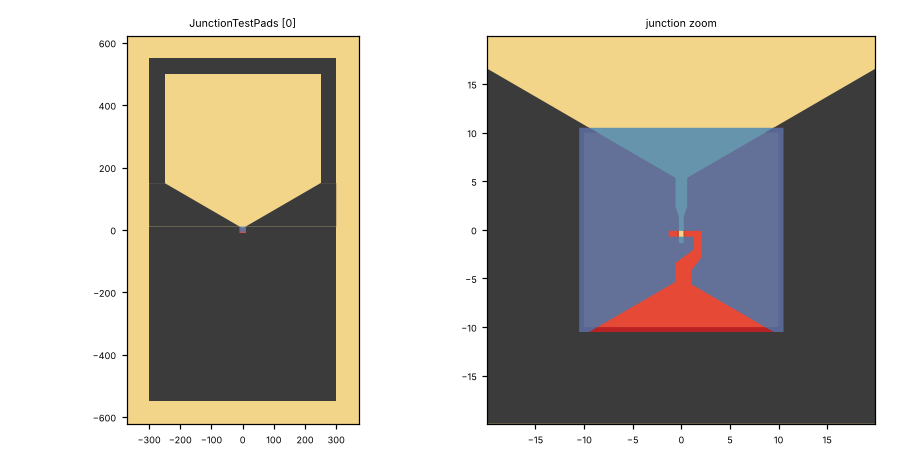
Pin image (default parameters). Light = metal, dark = etched gap, colours = junction layers. A red dot and arrow is a pin and its direction (out of the cell); the red bar is the CPW width a + 2 b. Blue dot = a pin without direction. Units: µm.
No pins: this cell has no ports. Place it with at= / rot=.
Notes from the catalog: the legacy QWri test-pad block (Quantcore). KQC’s test-structure factory of the same name is kqcircuits.test_structures.junction_test_pads.junction_test_pads.JunctionTestPads (dotted path).
Parameters
name |
default |
unit |
description |
|---|---|---|---|
|
|
μm |
Width of center conductor |
|
|
μm |
Width of gap |
|
|
μm |
Turn radius |
|
|
μm |
Upper pad width |
|
|
μm |
Upper pad height |
|
|
μm |
Lower pad width |
|
|
μm |
Lower pad height |
|
|
μm |
Upper pad shortened by (towards the window edge) |
|
|
μm |
Lower pad shortened by (towards the window edge) |
|
|
μm |
Junction window width |
|
|
μm |
Junction window height |
|
|
μm |
Pad tip distance from the junction |
|
|
μm |
Straight finger width |
|
|
μm |
Bent finger width |
|
|
μm |
Straight finger offset (legacy y) |
|
|
μm |
Straight finger lead width |
|
|
μm |
Straight finger length |
|
|
μm |
Bent finger offset (legacy x) |
|
|
μm |
Bent finger offset (legacy y) |
|
|
μm |
Bent finger lead width |
|
|
μm |
Bent finger length |
|
|
μm |
HSQ box width |
|
|
μm |
Label height |
|
|
μm |
Distance between the pads (junction region) |
|
|
μm |
Etch window wider than the upper pad by |
|
|
μm |
Etch window height (0 = pads + middle) |
|
|
μm |
Bent finger connection height |
|
|
– |
Draw HSQ sidewall boxes |
|
|
μm |
HSQ overlap onto the finger |
|
|
μm |
HSQ box centre offset (legacy y_off) |
|
|
μm |
HSQ box extra length below |
|
|
μm |
HSQ box extra length above |
|
|
– |
Spacer gradient: 51–53/0 dose levels inside the HSQ (width / 3 strips) |
|
|
– |
Text etched above the pads (empty = none) |
|
|
μm |
Label position [x, y] |
Electrically relevant parameters (sizes, gaps, junction, ports) come first, the rest follows.
LOM model
none (a LOM build gives each pin its own bare node, without elements).
How to use
In Python:
from quantcore_circuits.designer import Designer

d = Designer("demo", box=(0, 0, 7500, 7500))
d.add("U1", "JunctionTestPads", at=(3750, 3750), a=10)   # parameters: see the table above
# no directed pin: place it with at= / rot=, or snap it with snap= / to=
Pin names go into d.route(...) as INSTANCE.pin, and into snap= / to= when placing. From the shell: qcc components JunctionTestPads lists the pins; add --schema for the parameters.
In KLayout: Quantcore panel ▸ Components ▸ double-click the cell, then click on the layout to place it. Rotate and mirror before the click; use Connect on two pins to route.
GUI status (kplugin/COMPONENTS_STATUS.md): places ok, edit ok, connect n/a (no directed port), build ok. no ports.