Hackathon chip (Metal A.6)
Two pocket transmons with charge lines, 1.4 mm apart and joined by a short direct coupling line. Each qubit is read out by a λ/2 resonator through a three-finger series capacitor to an edge bond pad. It is the exercise chip of the Qiskit Metal hackathon (South Korea, 2020; Apache-2.0, © IBM and contributors). The Quantcore rebuild is distributed under GPL-3.0.
Build this one to learn readout through a series capacitor, a non-resonant coupling line between two qubits, and how charge lines enter a pocket from a pad on the die edge.
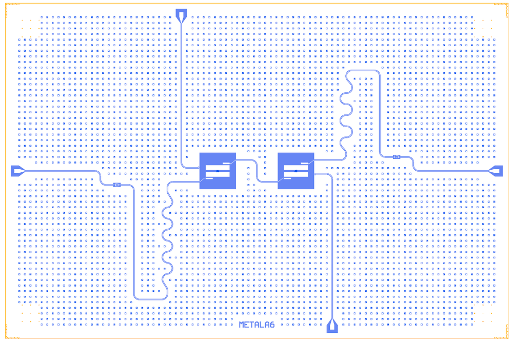
At a glance
Notebook |
|
Source |
Qiskit Metal |
Chip |
9 × 6 mm (the source’s size, larger than the 7.5 mm Quantcore die) |
On the chip |
2 pocket transmons with charge lines · 2 series capacitors · 2 λ/2 readouts (5 and 6 mm) · 1 direct coupling line · 2 charge lines · 4 bond pads |
Builds today |
yes (layout built on 2026-11-19 in 8 s) |
How the notebook builds it
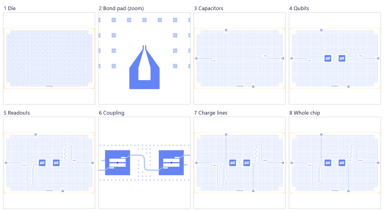
Die. An empty 9 × 6 mm chip with the QCT frame (dicing marks, alignment grids, chip boundary, device ID).
Bond pads. Readout and charge-line launchpads, slid to the 100 µm pad-edge rule (the picture zooms on one pad).
Capacitors. The two series capacitors and their lines to the readout pads.
Qubits. Two Metal pocket transmons with Quantcore junctions; the second is rotated 180°.
Readout resonators. Two λ/2 lines from the qubits through the capacitors, drawn as U-shapes.
Coupling. One short direct line between the two qubits’ bus pads.
Charge lines. One line from a south (Q1) and a north (Q2) launchpad into each charge pin.
Whole chip. Sim groups for the FEM jobs, the content centred in the die, the design saved.
LOM estimates
Numbers are from a run of this notebook on 2026-11-19 (Setup, Design, Check and the LOM cells, 9 s): QuCat normal modes with QuTiP dressed values.
group |
qubit |
f_q (GHz) |
α (MHz) |
resonator |
f_r (GHz) |
κ (MHz) |
χ (MHz) |
|---|---|---|---|---|---|---|---|
Q1+read |
Q1 |
6.96 |
-328 |
Readout_Q1 |
11.7 |
2.42 |
-1.63 |
Q2+read |
Q2 |
7.435 |
-311 |
Readout_Q2 |
9.867 |
1.47 |
-3.39 |
group |
pair |
ZZ (kHz) |
neighbours |
hybridised |
|---|---|---|---|---|
Q1+Q2+bus |
Q1-Q2 |
-6870 |
yes |
no |
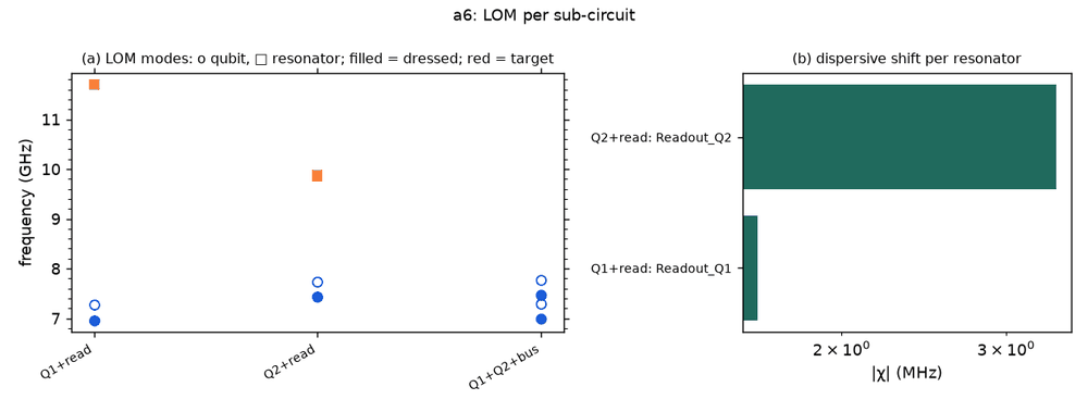
These are lumped-model estimates from component formulas and calibration, not FEM results. The LOM page says how far to trust them.
Build spec
The rest of this page is the detailed spec the notebook was built from: every component, port, route and length.
The
metal:references in this spec build as written, through themetal:wrapper (ports are the Metal pin names, parameters the Metal options). The Quantcore and KQC substitutions are optional.
Source: Quantum Metal docs/circuit-examples/full-design-flow-examples/A.6-Hackathon-exercise-South-Korea-2020.ipynb.
Licence Apache-2.0.
The chip has two TransmonPocketCL qubits 1.4 mm apart, joined by a short direct coupling line (non-resonant; the
LOM uses bus f = 0.1 GHz). Each qubit has a meander readout through a 3-finger Cap3Interdigital series cap to its
own edge pad, and a charge line from a top or bottom pad.
Chip: DesignPlanar default 9000 × 6000 µm, centred, so Designer = Metal + (4500, 3000). CPW 10/6 µm, fillet 99 µm.
The junctions are FakeJunction_01 (Q1) and FakeJunction_02 (Q2).
A first build uses these substitutions: Xmon for TransmonPocketCL, KQC FingerCapacitorSquare for
Cap3Interdigital, BondPad, free-end charge lines.
Components
Metal TransmonPocketCL options: pad_width 425, pocket_height 650, cl_pocket_edge 180 (cl_off_center 50 default); pads readout (+1, +1) and bus (−1, −1), both default 125 × 30.
instance |
catalog ref |
key params |
at (x, y) |
rot |
notes |
|---|---|---|---|---|---|
Q1 |
|
see above; hfss Lj 14 nH |
(5200, 3000) |
0 |
claw_n = readout (Metal pin (5625, 3195) E); claw_w = bus (Metal (4775, 2805) W); Metal CL pin (5617, 2945) E |
Q2 |
|
Lj 12 nH |
(3800, 3000) |
180 |
claw_n→S = readout (Metal (3375, 2805) W); claw_w→E = bus (Metal (4225, 3195) E); Metal CL (3383, 3055) W |
Cap_Q1 |
KQC |
trace 10 |
(7000, 3250) |
0 |
Metal a (6935, 3250) W ← resonator, b (7065, 3250) E → pad |
Cap_Q2 |
|
(2000, 2750) |
180 |
Metal a (2065, 2750) E ← resonator, b (1935, 2750) W → pad |
|
Launch_Q1_Read |
|
(7975, 3000) |
90 |
east edge |
|
Launch_Q2_Read |
|
(1025, 3000) |
270 |
west edge |
|
Launch_Q1_CL |
|
(5850, 525) |
0 |
south |
|
Launch_Q2_CL |
|
(3150, 5475) |
180 |
north |
Routes
route |
from → to |
type, length |
waypoints |
notes |
|---|---|---|---|---|
Bus_Q1_Q2 |
Q1.claw_w → Q2.claw_w |
cpw ≈ 855–900 |
— |
direct coupling line; Metal RoutePathfinder via (4475, 2805), (4475, 3195), end lead 250 |
Readout_Q1 |
Q1.claw_n → Cap_Q1.a |
meander 5000 |
— |
λ/2 (both ends capacitive); Metal lead 325/125, asym −50 |
Readout_Q2 |
Q2.claw_n → Cap_Q2.a |
meander 6000 |
— |
λ/2; same leads |
TL_Q1 |
Launch_Q1_Read.a → Cap_Q1.b |
cpw ≈ 1075 |
nodes [(7215, 3000), (7215, 3250)] |
end lead 150 |
TL_Q2 |
Launch_Q2_Read.a → Cap_Q2.b |
cpw ≈ 1075 |
nodes [(1785, 3000), (1785, 2750)] |
|
TL_Q1_CL |
Launch_Q1_CL.a → |
cpw ≈ 2611 |
nodes [(5850, 2945)] |
charge line approaches from the east |
TL_Q2_CL |
Launch_Q2_CL.a → |
cpw ≈ 2611 |
nodes [(3150, 3055)] |
from the west |
The FingerCapacitorSquare ports are a/b. Wire them so the resonator lands on the inner port and the pad route on
the outer port.
Launchers, pads, test structures, markers, labels
4 pads: 2 readout (E/W edges) and 2 charge (S, N). There are no markers.
LOM node structure
Q1 and Q2 are islands with JJs: Q1 Lj 14 nH, Q2 Lj 12 nH.
They are coupled directly through the bus line, which acts as a coupling capacitor network rather than a resonator.
Each qubit has a λ/2 readout with C_g at the claw and a series C (3-finger) to its 50 Ω port.
Each qubit has an open charge line with C_d.
Targets (if stated)
LOM setup (Q1): Lj 14 nH, Cj 2 fF, freq_readout 7.0 GHz, freq_bus [0.1, 0.1] (non-resonant). EPR sweep: Lj1 14 nH, Lj2 12 nH, 2 modes above 3 GHz. A 5 mm λ/2 readout sits near 12 GHz on Si, so lengths do not match the 7 GHz readout assumption. Retune with the LOM loop (about 8.4 mm for 7 GHz on Si, 9.0 mm on sapphire).
Simplifications for a first rebuild
Move the Xmon readout claw to north (Q1) and south (Q2), so the charge lines can approach on the open east/west sides at the Metal CL pin positions.
Make the direct bus a straight cpw between facing claws.
Quantcore PDK rebuild
The notebook is a Quantcore PDK rebuild of the source, not a replica: the netlist, LOM and imported components are kept, and the process is Quantcore’s.
Notebook: examples/designs/metal/a6_hackathon_2q.ipynb.
Chip: the Quantcore die frame (L dicing markers 1000/0, 3 × 3 alignment grids 1001/0, chip boundary 100/0, device ID where an edge is free; any brand text is QCT), drawn on the source’s 9 × 6 mm chip (the design does not fit the 7.5 mm die); no KQC chip frame.
Stack: sapphire 650 µm, εr 10.25 (the PDK default stack, used by the LOM estimates and every FEM export); Metal’s
DesignPlanardefault is silicon (εr 11.45, 750 µm), so the LOM capacitances, resonator frequencies and FEM jobs here are for sapphire rather than the source’s substrate.Junctions: Quantcore Nb/AlOx/Nb trilayer junctions (
junction_typefromlayouts.registry.trilayer_junction): fingers on 2/0 + 4/0, spacer 50/0 with the 51–53/0 gradient, sized on the PDK junction rule (Nb Δ = 1.4 meV, I_c·R_n = πΔ/2e, R_n·A 13.5 kΩ·µm² and C_J 50 fF/µm² assumed). The source detunes the qubits (hfss_inductance14 / 12 nH); the rebuild keeps that 14 : 12 ratio around the PDK nominal: Q1 L_J 7.32 nH (R_n 48.9 kΩ, C_J 13.8 fF), Q2 6.24 nH (41.7 kΩ, 16.2 fF), both in the 40–50 kΩ window. Expected f_q ≈ 6.9 / 7.4 GHz (estimates).Kept: the topology and every Metal component with the source’s options (through the
metal:wrapper), positions and orientations, every route’s end pins and total length, the sim groups (readouts 5.0 / 6.0 mm, the direct coupling line, the two charge lines).