TransmonTaperedInsets
Floating tapered-pad transmon in a filleted pocket (SQDMetal TransmonTaperedInsets).
Source: Quantcore. Category: qubit. Module: quantcore_circuits.layouts.qubits.sqdmetal_cells.
See also the catalog.
Pins
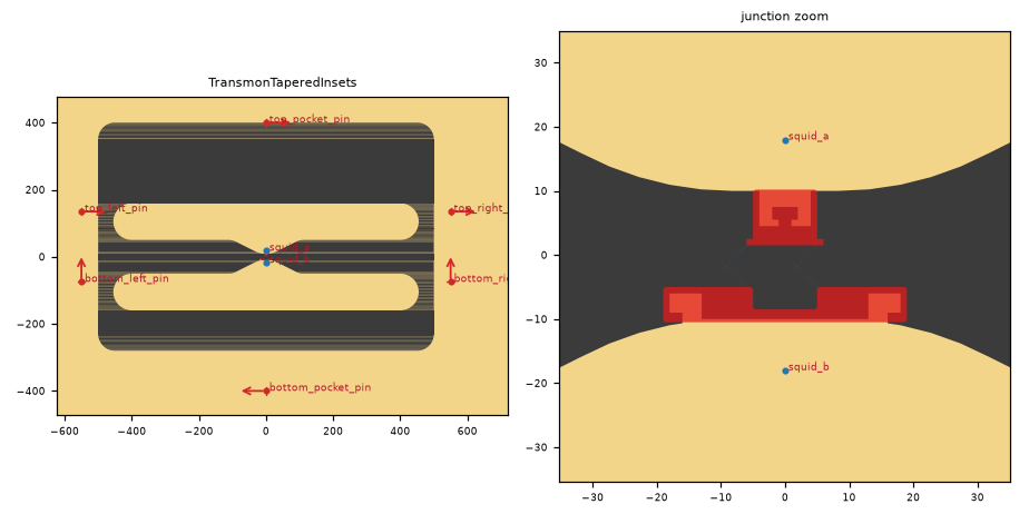
Pin image (default parameters). Light = metal, dark = etched gap, colours = junction layers. A red dot and arrow is a pin and its direction (out of the cell); the red bar is the CPW width a + 2 b. Blue dot = a pin without direction. Units: µm.
pin |
x (µm) |
y (µm) |
direction (°) |
a (µm) |
b (µm) |
purpose |
|---|---|---|---|---|---|---|
|
-550 |
-75 |
90 |
10 |
6 |
LOM node |
|
0 |
-400 |
180 |
10 |
6 |
grounded in the LOM |
|
550 |
-75 |
90 |
10 |
6 |
LOM node |
|
0 |
18 |
none |
10 |
6 |
junction pins (the LOM’s L_J); LOM node |
|
0 |
-18 |
none |
10 |
6 |
junction pins (the LOM’s L_J); LOM node |
|
-550 |
135 |
0 |
10 |
6 |
LOM node |
|
0 |
400 |
0 |
10 |
6 |
grounded in the LOM |
|
550 |
135 |
0 |
10 |
6 |
LOM node |
Pins with direction none: squid_a, squid_b. They mark a point (a junction lead, a pad centre), not a CPW end. The KLayout ghost draws them as boxes. A route can start there only where the notes say so; it cannot be snapped to.
a, b: CPW centre width and gap where the pin declares them (– = not declared). Position and direction are in the cell’s own frame (at=(0, 0), rot=0).
Notes from the catalog: SQDMetal TransmonTaperedInsets (Apache-2.0). The corner and pocket pins keep SQDMetal’s normals (top_pin +x, bottom_pin +y, top_pocket_pin +x, bottom_pocket_pin -x): placement marks in or at the pocket, not CPW ends. Connection-pad ports are CPW ends.
Parameters
name |
default |
unit |
description |
|---|---|---|---|
|
|
μm |
Width of center conductor |
|
|
μm |
Width of gap |
|
|
μm |
Turn radius |
|
|
– |
Mirror SQUID by its Y axis |
|
|
– |
Junction Type |
|
|
μm |
Junction width for code generated element |
|
|
μm |
Junction line width |
|
|
μm |
Junction line length |
|
|
μm |
Junction pins inset from the pad edge |
|
|
μm |
Gap between the pads |
|
|
μm |
Pad width (x, without the round ends) |
|
|
μm |
Pad height (y) |
|
|
μm |
Pocket width |
|
|
μm |
Taper width at the junction |
|
|
μm |
Taper width at the pad |
|
|
μm |
Taper height (0 = no taper) |
|
|
μm |
Taper corner radius |
|
|
– |
Junction position (SQDMetal junction_centered True / False / ‘left’) |
|
|
μm |
Junction offset from the pad end (right / left) |
|
|
μm |
Inset width (0 = none) |
|
|
μm |
Inset corner radius |
|
|
μm |
Pad fillet radius |
|
|
μm |
Pocket corner radius |
|
|
μm |
Coupler teeth height (0 = none) |
|
|
μm |
Coupler teeth width |
|
|
μm |
Gap between the coupler teeth |
|
|
– |
Connection pads (JSON {name: {options}}) |
|
|
– |
Junction cell parameters (JSON dict) |
|
|
μm^2 |
Loop area |
|
|
– |
Fluxline Type |
|
|
μm |
Corner pins: offset along y from the pad centre line |
|
|
μm |
Corner pins: offset along x from the pocket edge |
|
|
μm |
Pocket height |
|
|
μm |
Pocket shortened from below by |
|
|
μm |
Inset depth |
|
|
– |
Fillet points per quarter circle |
Electrically relevant parameters (sizes, gaps, junction, ports) come first, the rest follows.
LOM model
The cell contributes to the lumped model:
branch |
type |
nodes |
value (estimate at defaults) |
|---|---|---|---|
|
C |
island1 – gnd |
estimate=92.7, unit=fF, estimate_source=analytic: 910×110 µm pads across 100 µm in a 1000×800 µm pocket (coupled strips + CPW), estimate_kind=analytic, uncertainty=±25% |
|
C |
island2 – gnd |
estimate=106, unit=fF, estimate_source=analytic: 910×110 µm pads across 100 µm in a 1000×800 µm pocket (coupled strips + CPW), estimate_kind=analytic, uncertainty=±25% |
|
C |
island1 – island2 |
estimate=44.4, unit=fF, estimate_source=analytic: 910×110 µm pads across 100 µm in a 1000×800 µm pocket (coupled strips + CPW), estimate_kind=analytic, uncertainty=±25% |
|
SQUID |
island1 – island2 |
Lj_nH=6.734, Cj_fF=15, asym=0, flux_phi0=0 |
Nodes: island1, island2.
Simulation export notes
C1: Sim junction pads overlap / end on a curved island in a narrow gap (status: fixed; fix in layouts/junctions/sim_gap.py; layouts/qubits/qpdk_cells.py; layouts/qubits/sqdmetal_cells.py)
How to use
In Python:
from quantcore_circuits.designer import Designer

d = Designer("demo", box=(0, 0, 7500, 7500))
d.add("U1", "TransmonTaperedInsets", at=(3750, 3750), a=10)   # parameters: see the table above
d.add("PAD", "BondPad", at=(1125, 3750), rot=270)   # a launcher to connect to
d.route("L1", "PAD.a", "U1.bottom_left_pin")                # a CPW from the pad to the pin
Pin names go into d.route(...) as INSTANCE.pin, and into snap= / to= when placing. From the shell: qcc components TransmonTaperedInsets lists the pins; add --schema for the parameters.
In KLayout: Quantcore panel ▸ Components ▸ double-click the cell, then click on the layout to place it. Rotate and mirror before the click; use Connect on two pins to route.
GUI status (kplugin/COMPONENTS_STATUS.md): places ok, edit ok, connect ok, build ok. ports without direction: squid_a, squid_b (ghost draws boxes).