Full chip (Metal A.4)
A six-qubit teaching chip with a central hub qubit, a tunable coupler between two flux-tunable qubits, three flux lines and a multiplexed feedline along the north edge. It is the Qiskit Metal “A.4” full-chip example (Apache-2.0, © IBM and contributors), whose resonator lengths are only roughly chosen. The Quantcore rebuild is distributed under GPL-3.0.
Build this one to see a whole processor-style chip assembled in the order a designer would draw it: feedline, qubits, readout, coupling, then flux lines. It mixes five component types and shows tunable coupling, series-capacitor readout and multiplexed readout in one layout.
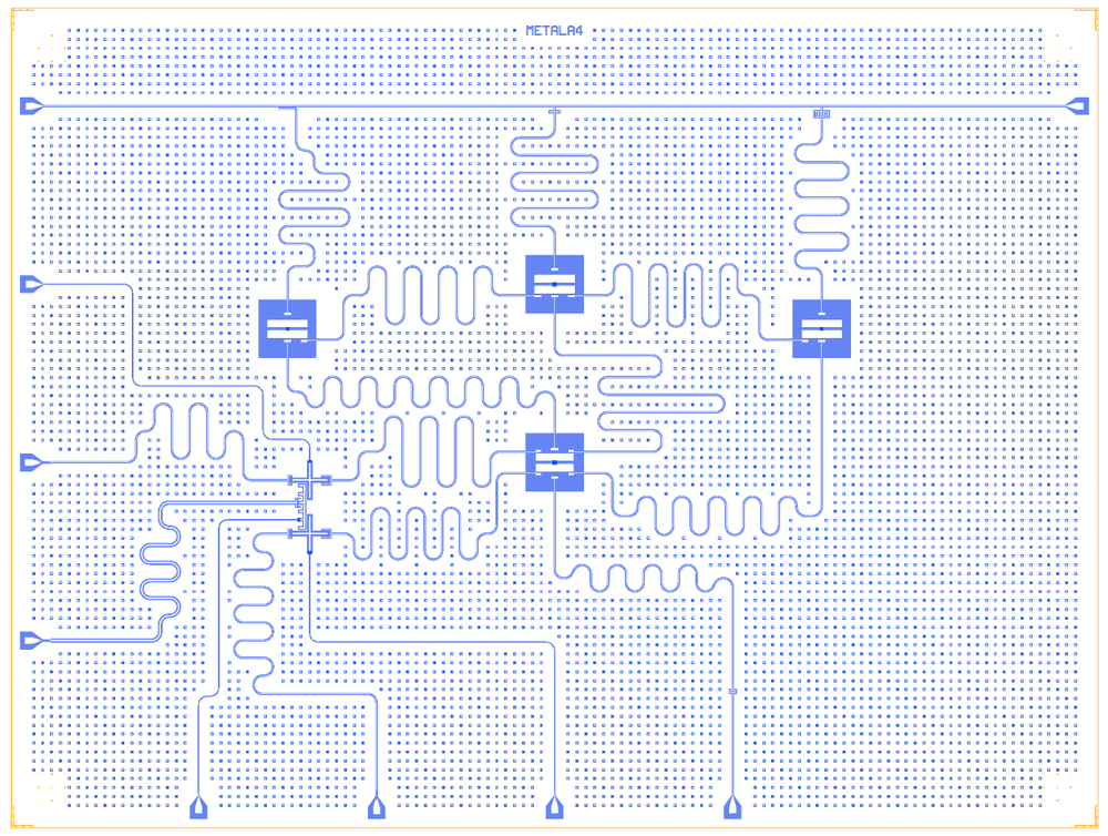
At a glance
Notebook |
|
Source |
Qiskit Metal |
Chip |
12.2 × 9.2 mm (the source’s 11 × 8 mm grown by 0.6 mm per side), CPW 10 / 6 µm, flux lines 5 / 3 µm |
On the chip |
6 qubits (hub |
Builds today |
yes (layout built on 2026-11-19 in 14 s) |
How the notebook builds it
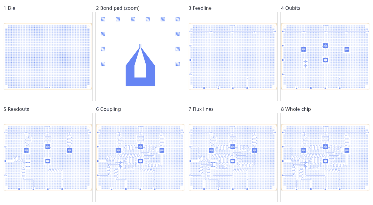
Die. An empty chip with the QCT frame (dicing marks, alignment grids, chip boundary, device ID).
Bond pads. Nine launchpads on the south, west and east edges, slid to the 100 µm pad-edge rule (the picture zooms on one pad).
Feedline. The north feedline with three tees and the series capacitor of the hub qubit.
Qubits. Six qubits, each with a Quantcore trilayer junction, and the tunable coupler with its SQUID.
Readout resonators. Six fixed-length resonators, one λ/4 and five λ/2, to the feedline tees, the capacitor and the coupled pads.
Coupling. The tunable coupler between the two crossmons and the seven buses around the hub.
Flux lines. Three 5 / 3 µm lines to the two crossmons and the coupler.
Whole chip. The target for the hub qubit, sim groups for the FEM jobs, the content centred in the die, the design saved.
LOM estimates
Numbers are from a run of this notebook on 2026-11-19 (Setup, Design, Check and the LOM cells, 31 s): QuCat normal modes with QuTiP dressed values.
group |
qubit |
f_q (GHz) |
α (MHz) |
resonator |
f_r (GHz) |
κ (MHz) |
χ (MHz) |
|---|---|---|---|---|---|---|---|
Q_Main+read |
Q_Main |
4.977 |
-376 |
Read_Q_Main |
10.49 |
2.05 |
-0.181 |
Q1+read |
Q1 |
5.787 |
-199 |
Read_Q1 |
8.864 |
5.58 |
-0.016 |
Q2+read |
Q2 |
5.787 |
-199 |
Read_Q2 |
11.04 |
10.7 |
-0.0102 |
TC+read |
Tune_C_Q12 |
8.334 |
-440 |
Read_TuneC |
10.55 |
9.32 |
-6.78 |
Q3+read |
Q3 |
7.197 |
-319 |
Q3_Read_T |
5.665 |
0.0876 |
-0.98 |
Q4+read |
Q4 |
7.093 |
-310 |
Read_Q4 |
10.23 |
4.21 |
-0.513 |
Q5+read |
Q5 |
7.193 |
-320 |
Read_Q5 |
10.7 |
37.4 |
-0.429 |
group |
pair |
ZZ (kHz) |
neighbours |
hybridised |
|---|---|---|---|---|
Q_Main+Bus_01+Q1 |
Q1-Q_Main |
-0.108 |
yes |
no |
Q_Main+Bus_02+Q2 |
Q2-Q_Main |
-0.133 |
yes |
no |
Q_Main+Bus_03+Q3 |
Q3-Q_Main |
-1.43 |
yes |
no |
Q_Main+Bus_04+Q4 |
Q4-Q_Main |
-1.52 |
yes |
no |
Q_Main+Bus_05+Q5 |
Q5-Q_Main |
-6 |
yes |
no |
Q3+Bus_Q3_Q4+Q4 |
Q3-Q4 |
46.9 |
yes |
no |
Q4+Bus_Q4_Q5+Q5 |
Q4-Q5 |
75 |
yes |
no |
Q1+TC+Q2 |
Q1-Q2 |
– |
no |
yes |
Q1+TC+Q2 |
Q1-Tune_C_Q12 |
– |
yes |
yes |
Q1+TC+Q2 |
Q2-Tune_C_Q12 |
– |
yes |
yes |
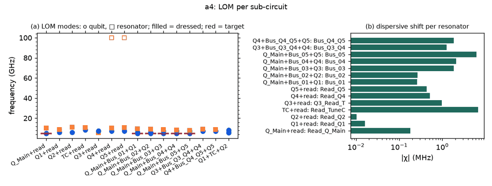
These are lumped-model estimates from component formulas and calibration, not FEM results. The LOM page says how far to trust them.
Build spec
The rest of this page is the detailed spec the notebook was built from: every component, port, route and length.
The
metal:references in this spec build as written, through themetal:wrapper (ports are the Metal pin names, parameters the Metal options). The Quantcore and KQC substitutions are optional. The full chip builds withmetal:TransmonPocket6,metal:TunableCoupler01(pinsControl/Flux) andmetal:CapNInterdigitalTee; subset A below is the quickest first build.
Source: Quantum Metal docs/circuit-examples/full-design-flow-examples/A.4-Full-chip-design.ipynb. Licence
Apache-2.0. It is a teaching layout (“resonator lengths only roughly chosen”) that is taken through Q3D/Elmer LOM,
HFSS EPR and GDS.
Q_Main is a TransmonPocket6 with 6 pads, bused to five qubits. Q1 and Q2 are TransmonCrossFL with flux lines,
coupled through a TunableCoupler01. Q3, Q4 and Q5 are TransmonPocket6 in a bus chain and are multiplexed on a
north feedline through a CoupledLineTee (λ/4) and two CapNInterdigitalTee (λ/2). Q_Main, Q1, Q2 and TC are each read
out separately.
Chip 11 000 × 8000 µm, centred at (0, −0.5) mm, so Designer = Metal + (5500, 4500). CPW 10/6 µm; flux lines 5/3 µm.
Fillet 99 µm. The junctions are FakeJunction_01 cells.
Q_Main needs 6 couplers and Q4 needs 4, and no Quantcore/KQC qubit has more than 3, so the full chip needs
metal:TransmonPocket6 and metal:TunableCoupler01. The north block (subset A below) builds from Quantcore and KQC parts.
Components
TransmonPocket6 base: pads 455 × 90, pad_gap 30, pocket 650 × 650. Connection pads at loc_W 0 have vertical pins at (0, ±425); those at loc_W ±1 have pins at (±425, ±120).
instance |
catalog ref |
key params (µm) |
at (x, y) |
rot |
pins (Designer frame) |
|---|---|---|---|---|---|
Q_Main |
metal:TransmonPocket6 |
pad_width 425, pocket_height 650; readout (0, −1, w 80, gap 50); bus_01 (−1, −1, 60, 10); bus_02 (−1, +1, 60, 10); bus_03 (0, +1, 90, 30); bus_04 (+1, +1, 60, 10); bus_05 (+1, −1, 60, 10); hfss Lj 14 nH |
(5500, 3500) |
0 |
readout (5500, 3075) S; bus_01 (5075, 3380) W; bus_02 (5075, 3620) W; bus_03 (5500, 3925) N; bus_04 (5925, 3620) E; bus_05 (5925, 3380) E |
Q1 |
|
bus_01 claw E, claw_length 95; readout claw W |
(2750, 2700) |
0 |
Metal bus_01 (3031, 2700) E, readout (2469, 2700) W, flux (2750, 2441.5) S |
Q2 |
|
bus_02 claw (Metal loc 0 → E after 180°), claw_length 95 |
(2750, 3300) |
180 |
Metal bus_02 (3031, 3300) E, readout (2469, 3300) W, flux (2750, 3558.5) N |
Tune_C_Q12 |
metal:TunableCoupler01 |
c_width 500 (others default: l_width 20, l_gap 10, a_height 60, fl 5/3/10) |
(2690, 3000) |
90 |
Control (2596, 3048) W, Flux (2602.5, 2856) W |
Q3 |
metal:TransmonPocket6, or |
bus_03 (0, −1, 80, 15), bus_q3_q4 (+1, −1, 80, 15), readout (0, +1, 80, 50); Lj 14 nH |
(2500, 5000) |
0 |
bus_03 (2500, 4575) S, bus_q3_q4 (2925, 4875) E, readout (2500, 5425) N |
Q4 |
metal:TransmonPocket6, or |
bus_04 (0, −1), bus_q3_q4 (−1, −1), bus_q4_q5 (+1, −1), readout (0, +1, 80, 50) |
(5500, 5500) |
0 |
bus_04 (5500, 5075) S, q3_q4 (5075, 5375) W, q4_q5 (5925, 5375) E, readout (5500, 5925) N |
Q5 |
metal:TransmonPocket6, or |
bus_05 (0, −1), bus_q4_q5 (−1, −1), readout (0, +1) |
(8500, 5000) |
0 |
bus_05 (8500, 4575) S, q4_q5 (8075, 4875) W, readout (8500, 5425) N |
Read_Q_Main_Cap |
KQC |
(7500, 927) |
90 |
Metal north_end (7500, 1000), south_end (7500, 854) |
|
Q3_Read_T |
hanger (metal:CoupledLineTee) |
coupling_length 200, space 3, down 100, short |
centre (2500, 7500) |
— |
λ/4 |
Q4_Read_T |
hanger |
finger_length 0, 8 fingers (gap cap, ~122 µm wide) |
centre (5500, 7500) |
— |
λ/2 |
Q5_Read_T |
hanger |
finger_length 50, 11 fingers (~170 µm) |
centre (8500, 7500) |
— |
λ/2 |
pads |
|
QMain_Read (7500, 525) r0; Q1_FL (5500, 525) r0 (5/3); Q1_Read* (3500, 500) r0, cap (3500, 595); TuneC_FL (1500, 525) r0 (5/3); TuneC_Read* (500, 1500) r270, cap (595, 1500); Q2_Read* (500, 3500) r270, cap (595, 3500); Q2_FL (525, 5500) r270 (5/3); NW (525, 7500) r270; NE (10475, 7500) r90 |
* = LaunchpadWirebondCoupled |
Routes
route |
from → to |
type, length |
waypoints / hanger |
notes |
|---|---|---|---|---|
Bus_01 … Bus_05 |
Q_Main.bus_0k → Q1.bus_01 / Q2.bus_02 / Q3.bus_03 / Q4.bus_04 / Q5.bus_05 |
meander 6000, 6400, 6800, 7200, 7600 |
— |
Metal asym 1305 (spacing 250), 450, 50, 150 (start jogs L250, R200), 50. EPR retunes Bus_05 to 7500 |
Bus_Q3_Q4, Bus_Q4_Q5 |
Q3→Q4, Q4→Q5 |
meander 6400, 6800 |
— |
lead 125/125, 125/25 |
Read_Q_Main |
Q_Main.readout → Read_Q_Main_Cap (north port) |
meander 5600 |
— |
λ/2; Metal lead 725/625, jogs L250 / end L600 |
Read_Q_Main_Cap_Launch |
cap (south port) → Launch_QMain_Read.a |
cpw ≈ 330 |
— |
|
Read_Q1, Read_Q2 |
Q1 readout claw → cap at Launch_Q1_Read; Q2 → cap at Launch_Q2_Read |
meander 6800, 5400 |
— |
λ/2; Read_Q2 asym −450 |
Read_TuneC |
TC.Control → cap at Launch_TuneC_Read |
meander 5800 |
— |
start lead 1525 |
Flux_Line_Q1 |
Launch_Q1_FL.a → Q1.flux |
cpw 4582, a 5 b 3 |
nodes [(5500, 1483), (2750, 1483)] |
Metal RoutePathfinder, reversed |
Flux_Line_TuneC |
Launch_TuneC_FL.a → TC.Flux |
cpw 3306, 5/3 |
[(1500, 875), (1728, 875), (1728, 2856)] |
|
Flux_Line_Q2 |
Launch_Q2_FL.a → Q2.flux |
cpw 3954, 5/3 |
[(675, 5500), (675, 4358), (2225, 4358), (2225, 3734), (2750, 3734)] |
|
FL_N |
Launch_NW.a → Launch_NE.a |
cpw 9950, straight y = 7500 |
— |
north mux feedline (Metal ML_TL_01…04 through the three tees) |
Read_Q3 |
Q3 readout → |
meander 5300 |
— |
Metal 5000 + 300 tee |
Read_Q4 |
Q4 readout → |
meander ≈ 5900 |
— |
Metal 5800 + tee |
Read_Q5 |
Q5 readout → |
meander ≈ 5600 |
— |
Metal 5400 + tee |
Launchers, pads, test structures, markers, labels
11 pads: 4 on the south edge (QMain_Read, Q1_FL, Q1_Read*, TuneC_FL), 3 on the west (TuneC_Read*, Q2_Read*, Q2_FL), and NW/NE on the north feedline. There are no markers.
LOM node structure
Q_Main is the hub. It has a C_g to each of the 5 λ/2 buses: Q1 (5.6 GHz), Q2 (5.7), Q3 (5.8), Q4 (5.9), Q5 (6.0 per the LOM setup).
Q3–Q4–Q5 form a bus chain. Q1 and Q2 are coupled through TC (a SQUID island).
Readouts: R_QMain is λ/2 with a series C to its port. R_Q1, R_Q2 and R_TC are λ/2 with coupled-pad C to their ports. R_Q3 is λ/4 (hanger short) on FL_N. R_Q4 and R_Q5 are λ/2 with tee C on FL_N.
Flux bias on Q1, Q2 and TC.
Targets (if stated)
Q_Main LOM setup: Lj 14 nH, Cj 2 fF, readout 7.0 GHz, buses [5.6, 5.7, 5.8, 5.9, 6.0] GHz. The Q3D + LOM result quoted in the text is f_Q 4.96 GHz, α −351 MHz, g 44–52 MHz.
Q3D C reference: readout pad 42.1 fF, pad_top 97.5 fF, pad_top–pad_bot −31.2 fF.
EPR run: Lj(Q_Main) 13 nH, Lj(Q5) 15 nH, Bus_05 7.5 mm. Q3–Q5 Lj 14 nH; Q1/Q2 Metal default 10 nH.
Simplifications for a first rebuild
Subset A: FL_N with Q3/Q4/Q5 as Xmon (claw_n = readout; e/w = chain buses), Bus_Q3_Q4, Bus_Q4_Q5, and Read_Q3–Q5. This is a 3-qubit mux test of hanger readout with both short and open ends.
Full chip: use
metal:TransmonPocket6andmetal:TunableCoupler01. For the open tees, use a hangerend="open"or, more faithfully, a KQCWaveguideCoplanarSplitterplusFingerCapacitorSquare.Every coupled launchpad becomes a BondPad plus a FingerCapacitorSquare at the Metal tie pin.
Quantcore PDK rebuild
The notebook is a Quantcore PDK rebuild of the source, not a replica: the netlist, LOM and imported components are kept, and the process is Quantcore’s.
Notebook: examples/designs/metal/a4_full_chip.ipynb.
Chip: the Quantcore die frame (L dicing markers 1000/0, 3 × 3 alignment grids 1001/0, chip boundary 100/0, device ID where an edge is free; any brand text is QCT), on the source’s 11 × 8 mm chip grown by 0.6 mm on every side (box
(-600, -600, 11600, 8600)) so that the corner launchpadsLaunch_NW/Launch_NEand the feedline clear the PDK marker areas; every coordinate stays the source’s.Stack: sapphire 650 µm, εr 10.25 (the PDK default stack, used by the LOM estimates and every FEM export); Metal’s
DesignPlanardefault is silicon (εr 11.45, 750 µm), so the LOM capacitances, resonator frequencies and FEM jobs here are for sapphire rather than the source’s substrate.Junctions: Quantcore Nb/AlOx/Nb trilayer junctions (
junction_typefromlayouts.registry.trilayer_junction): fingers on 2/0 + 4/0, spacer 50/0 with the 51–53/0 gradient, sized on the PDK junction rule (Nb Δ = 1.4 meV, I_c·R_n = πΔ/2e, R_n·A 13.5 kΩ·µm² and C_J 50 fF/µm² assumed).Q_Mainis sized for the tutorial’s f_q 4.96 GHz (its C_Σ ≈ 55 fF from the LOM): straight finger 0.23 µm × 0.6 µm, L_J 14.6 nH, C_J 6.9 fF, so R_n ≈ 98 kΩ, above the 40–50 kΩ window (a 45 kΩ junction would put this small pocket at ≈ 7.1 GHz).Q3–Q5get the PDK nominal junction, 0.5 × 0.6 µm fingers → R_n = 45 kΩ, L_J = 6.73 nH, C_J = 15 fF (in the 40–50 kΩ window) (expected ≈ 7.1–7.6 GHz).Q1,Q2and the coupler (flux lines) get a PDK SQUID of two 0.25 × 0.6 µm junctions → R_n = 45 kΩ in parallel, L_J = 6.73 nH at zero flux, C_J = 15 fF (in the 40–50 kΩ window); expectedQ1/Q2≈ 5.8 GHz, the coupler ≈ 8.3 GHz at zero flux (above the 4–8 GHz band; it is flux-tuned down).Kept: the topology and every Metal component with the source’s options (through the
metal:wrapper), positions and orientations, every route’s end pins and total length, the sim groups (buses 6.0–7.6 mm, readouts 5.0–6.8 mm, the three flux-line paths, thed.couplecoupler estimates).