Gatemon test chip (QPDK)
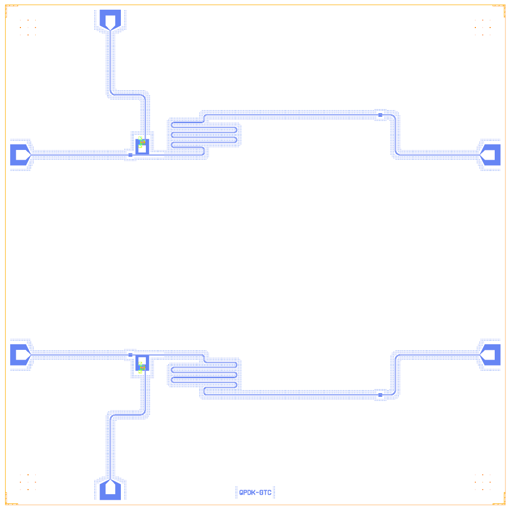
Two carbon-nanotube gatemons, each coupled to its own λ/2 resonator that is measured in transmission, plus a gate line per gatemon. The layout comes from QPDK’s gatemon_test_chip.pic.yml (MIT; after Riechert et al., Nat. Commun. 2025) and is rebuilt on the Quantcore PDK; the rebuild is GPL-3.0.
This notebook is an example of a resonator measured in transmission (IDC, coupler, meander, IDC), of the Quantcore Gatemon cell, and of a chip bigger than the standard die.
At a glance
Notebook |
|
Source |
gdsfactory |
Chip |
10 × 10 mm (the source’s size, larger than the 7.5 mm die), CPW 10 / 6 µm |
On the chip |
6 launchers · 2 gatemons · 2 gatemon couplers · 2 λ/2 resonators (11946 µm) · 4 series IDCs · 2 gate lines |
Builds today |
yes (layout built on 2026-11-19 in 5 s) |
How the notebook builds it
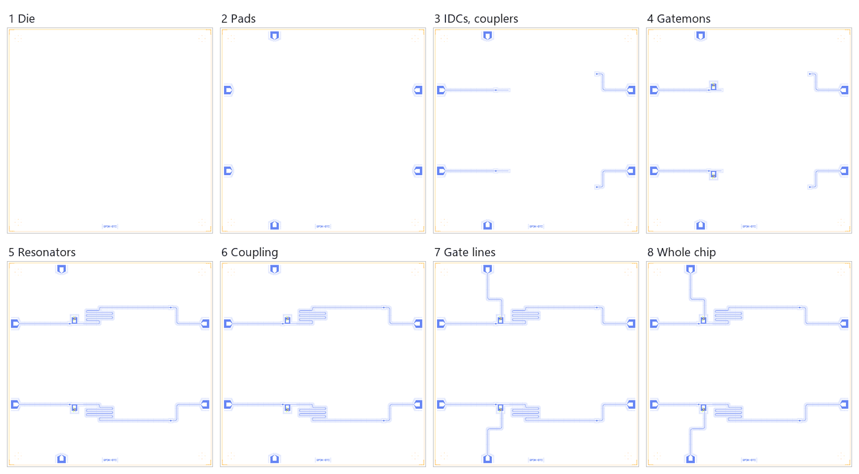
Die. The 10 × 10 mm chip with the frame and the device ID.
Bond pads. Six launchers.
IDCs and couplers. Per channel the input and output IDCs, the gatemon coupler and the leads.
Gatemons. Two
Gatemoncells at the coupler.Resonators. The rest of each λ/2, from the coupler to the output IDC.
Coupling. The declared gatemon-to-resonator connection (the channels do not couple to each other).
Gate lines. One gate CPW per gatemon to its own launcher.
Whole chip. Sim groups, targets from the source, centring, save.
LOM estimates
Numbers are from a run of this notebook on 2026-11-19 (Setup, Design, Check and the LOM cells, 6 s): QuCat normal modes with QuTiP dressed values.
group |
qubit |
f_q (GHz) |
α (MHz) |
resonator |
f_r (GHz) |
κ (MHz) |
χ (MHz) |
|---|---|---|---|---|---|---|---|
CH_A |
G_A |
4.328 |
-421 |
– |
– |
– |
– |
CH_B |
G_B |
4.328 |
-421 |
– |
– |
– |
– |
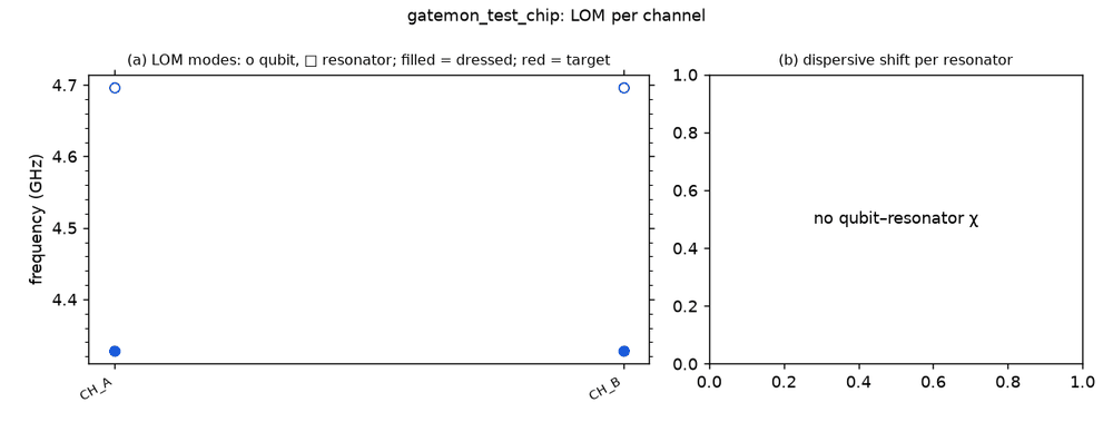
These are lumped-model estimates (component formulas and calibration), not FEM results. The LOM page says how far to trust them.
Build spec
The rest of this page is the detailed spec the notebook was built from, with every component, port, route and length.
Source: qpdk/samples/gatemon_test_chip.pic.yml
· cells qpdk/cells/gatemon.py (gatemon, gatemon_coupler) · licence MIT (verified) · Read on 2026-11-02.
Reference (in the YAML info): Riechert et al., carbon-nanotube gatemon, Nat. Commun. 2025,
https://doi.org/10.1038/s41467-025-62283-y. Image: docs/_static/images/gatemon_test_chip.png (filled).
What it is: two independent channels (a = south, b = north, mirror images). Each channel runs launcher → series IDC →
600 µm coupler straight (the gatemon island couples here, 200 µm from its start) → 9946 µm meander → 1400 µm tail →
series IDC → launcher. That is a half-wave resonator in transmission, 11946 µm total. Each gatemon also has a gate
electrode routed to its own launcher.
Frame: source centred on (0, 0); launchers at ±4850. The filled version’s chip edge is about 9930 × 9900 µm.
Use box (0, 0, 10000, 10000), Designer = source + (5000, 5000). Si, M1 negative. The YAML info gives the
gatemon layer stack (hBN εr 3.4, CNT, Nb/Au contacts).
The first version used a plain Swissmon stand-in for the gatemon (below); the rebuild uses the Gatemon and GatemonCoupler cells.
Components
instance |
catalog ref |
key params (units) |
at (x, y) Designer |
rot |
notes |
|---|---|---|---|---|---|
PIN_A / PIN_B |
|
default |
(150, 3000) / (150, 7000) |
270 (faces east) |
launcher_in_a/b (−4850, ∓2000) |
POUT_A / POUT_B |
|
default |
(9850, 3000) / (9850, 7000) |
90 (faces west) |
launcher_out_a/b (4850, ∓2000) rot 180 |
PG_A |
|
default |
(2600, 150) |
0 (faces north) |
launcher_gate_a (−2400, −4850) rot 90 |
PG_B |
|
default |
(2600, 9850) |
180 (faces south) |
launcher_gate_b (−2400, 4850) rot −90 |
CI_A / CI_B |
|
4 fingers, 20 long, 2 gap, 5 wide |
(3000, 3000) / (3000, 7000) |
0 |
cap_in_a/b (−2000, ∓2000) |
CO_A / CO_B |
|
same |
end of tail, ≈ (8320, 2200) / (8320, 7800) |
0 |
cap_out_a/b, placed by connection |
G_A |
|
island_size (150, 150), pocket_gap 60, pocket_gap_top 40, electrode_size (60, 60), electrode_spacing 100, junction_length 1 (CNT weak link), hbn_size (80, 80), gate_tip_width 16, gate_tip_gap 5, gate_length 50 |
(3218, 2880) |
0 |
gatemon_a (−1782, −2120); readout side faces the line (+y) |
G_B |
same |
same |
(3218, 7120) |
mirrored (readout faces −y) |
gatemon_b (−1782, 2120) mirror |
K_A / K_B |
|
length 600, coupling_position 200, island_width 150, pocket_gap_top 40, coupling_capacitance 5.4 fF; K_B qubit_side top |
connected to CI_x.b |
0 |
a passing CPW with a capacitive island port |
Routes
route |
from → to |
type, length |
waypoints |
notes |
|---|---|---|---|---|
IN_A / IN_B |
PIN_x.a → CI_x.a |
cpw |
straight y 3000 / 7000 |
probeline_input |
RES_A |
CI_A.b → CO_A.a |
meander 11946 (600 coupler + 9946.135 meander, 4 meanders + 1400 tail) |
coupler straight east from x ≈ 3030, meander south of y 3000 down to y ≈ 2200, tail east along y 2200 |
λ/2; source resonator_a, open_start/open_end false (continuous) |
RES_B |
CI_B.b → CO_B.a |
meander 11946 |
mirror: north of y 7000, tail along y 7800 |
resonator_b mirror |
OUT_A |
CO_A.b → POUT_A.a |
cpw |
nodes (8300, 2200), (8300, 3000) |
probeline_output_a waypoints (3300, −2800), (3300, −2000) |
OUT_B |
CO_B.b → POUT_B.a |
cpw |
nodes (8300, 7800), (8300, 7000) |
|
GATE_A |
G_A.gate → PG_A.a |
cpw |
nodes (3278, 1800), (2600, 1800) |
gate_line_a waypoints (−1722, −3200), (−2400, −3200) |
GATE_B |
G_B.gate → PG_B.a |
cpw |
nodes (3278, 8200), (2600, 8200) |
The qubit is not on a hanger. G_x sits in a pocket beside the first straight of RES_x. Our route model has no
“pad-beside-route” coupling, so RES_x must be split at the coupling point (needs gatemon_coupler).
Launchers, pads, test structures, markers, labels
6 launchers. The filled variant (filled_gatemon_test_chip) adds a chip edge and 15 µm vortex fill.
LOM node structure
G_x: one island node with C_Σ (target E_C/h = 260 MHz, so C_Σ ≈ 75 fF), and a gate-tunable CNT junction to ground (Lj tunable, no SQUID). C_g ≈ 5.4 fF to the resonator’s input-end node.
RES_x: λ/2 CPW between two series IDCs (C_in, C_out), ports PIN_x and POUT_x. The qubit couples near the input voltage antinode.
GATE_x: DC gate control on G_x (sets Ej). No flux lines, no bus. Channels a and b are independent.
Targets (YAML info)
readout_target 5.056 GHz (device A bare cavity, both channels) · E_C 260 MHz · g 50 MHz · coupling capacitance 5.4 fF. These are calibrated with QPDK analytical CPW and capacitor models (junction open), not FEM. Check: λ/2 at 5.056 GHz on Si (ε_eff 6.2) is 11.9 mm, matching 11946 µm.
Simplifications for a first rebuild
Stand-in qubit:
Swissmon(one arm toward RES_x) orDoublePads, withjunction={"Lj_nH": 20}(assumed; about 3.9 GHz at E_C 260 MHz). Place it at G_x and model the gate line as a drive line ending near the island (free_end).Treat RES_x as a fixed-length cpw route from CI_x.b to CO_x.a (
meander=11946). The capacitive qubit tap then needs eithergatemon_coupleror a short stub, a hanger withend="open", from the qubit coupler to RES_x near s ≈ 200.The components gatemon (pocketed 150 µm island with CNT weak link, hBN, top gate; ports
readout,gate) and gatemon_coupler (600 µm through-CPW with an island-coupling port at 200 µm, C ≈ 5.4 fF) are needed for the real thing.
First build
The first version of examples/designs/qpdk/gatemon_test_chip.ipynb used a KQC Swissmon 150 µm square island stand-in (Lj 20 nH assumed) beside the plain resonator straight, coupling declared as couple(C_fF=5.4) to CI_x.b (a coupling that names a route breaks the C-matrix export). CO_x moved to source x 3000 so the output route can turn at x 3300.
Rebuild with Gatemon + GatemonCoupler
The Swissmon stand-in is replaced: K_x = GatemonCoupler(length 600, qubit_side bottom|top) snapped o1 → CI_x.b (QPDK
connection), G_A = Gatemon snapped readout → K_A.qubit; G_B is mirrored in QPDK, and Designer.add drops
mirror with a snap, so it is placed explicitly (mirror, on K_B.qubit) with a wire coupling. Gate routes go to
G_x.gate via the QPDK waypoints. The KQC IDC is 37 µm longer than QPDK’s, so coupler, gatemon and the last gate
waypoint sit 18.5 µm east of the source. λ/2 = 600 + 11346.1 µm route. LOM: f_q 4.33 GHz, α −421 MHz (target −260;
lom’s analytic island C 51 fF vs QPDK’s 75 fF; was −1014 with the stand-in), Lj 20 nH assumed. Open issue: the λ/2 is
missing from the LOM (the coupler line and the meander route between the IDCs resolve to a wire).
Quantcore PDK rebuild
The notebook is a Quantcore PDK rebuild, not a replica: the netlist, LOM and imported components are kept, the process is Quantcore’s.
Notebook: examples/designs/qpdk/gatemon_test_chip.ipynb.
Chip: the Quantcore die frame (L dicing markers 1000/0, 3 × 3 alignment grids 1001/0, chip boundary 100/0, device ID where an edge is free; any brand text is QCT), drawn on the source’s 10 × 10 mm chip (the design does not fit the 7.5 mm die); no KQC chip frame.
Stack: sapphire 650 µm, εr 10.25 (the PDK default stack, used by the LOM estimates and every FEM export); QPDK’s process is Al on Si (εr 11.45), so frequencies are not the QPDK ones.
Junctions: there is no Josephson tunnel junction to replace. The gatemon’s weak link is a gate-tunable carbon nanotube, so no Quantcore trilayer junction applies, and its contacts / CNT / hBN / Al patch / top gate have no PDK v3 fab layer (not drawn, as before). The LOM keeps the assumed fixed Lj = 20 nH, Cj = 2 fF.
Kept: the topology and every component with the source’s parameters and positions, the readout / resonator lengths and coupled sections, the sim groups (the 11946 µm λ/2 between the IDCs, the 5.4 fF coupling, the YAML targets).