Wallraff 17-qubit (Metal 53)
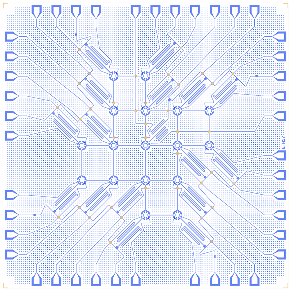
The ETH Zurich distance-3 surface-code device: 17 flux-tunable star transmons (9 data, 8 auxiliary) on a lattice, 24 nearest-neighbour couplers, and per qubit a λ/4 readout resonator with its own Purcell filter, read out on four feedlines. The layout is the Qiskit Metal “53” mock-up (Apache-2.0, © Qiskit Metal contributors), traced from micrographs of Krinner et al. (Nature 605, 669, 2022): a mock-up, not a mask. The Quantcore rebuild is distributed under GPL-3.0.
Build this one to see a full 17-qubit chip built from a generator, with every part drawn through the same Designer steps as the small chips. It takes about half a minute to build.
At a glance
Notebook |
|
Source |
Qiskit Metal |
Chip |
14.4 × 14.4 mm |
On the chip |
17 star transmons · 24 couplers · 17 readout and 17 Purcell λ/4 resonators · 4 feedlines · 17 Z and 17 XY lines · bond pads on the used slots of 48 |
Builds today |
yes (layout built on 2026-11-19 in 33 s) |
How the notebook builds it
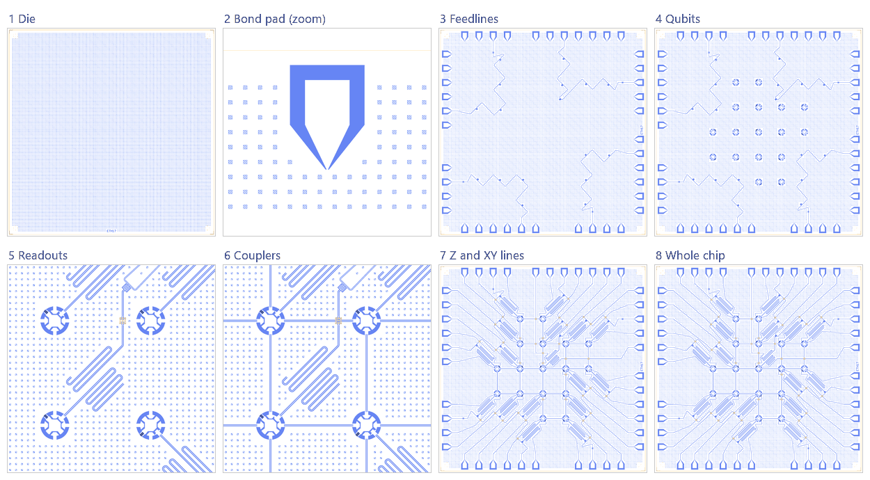
Die. An empty 14.4 mm square with the QCT frame, the lattice centre at the die centre.
Bond pads. The generator’s pads, slid to the 100 µm pad-edge rule (the picture zooms on one pad).
Feedlines. The four feedlines with their interdigital tees and input capacitors.
Qubits. Seventeen
StarQubittransmons, each with a PDK SQUID (the picture zooms on the centre of the lattice).Readout resonators. A readout λ/4 and a Purcell λ/4 per qubit (zoom).
Couplers. The 24 nearest-neighbour coupler lines (zoom).
Z and XY lines. The flux and drive lines from the pads to every qubit.
Whole chip. The qubit targets, sim groups for the FEM jobs, the content centred in the die, the design saved.
LOM estimates
Numbers are from the saved output of the .v1 notebook (the 17-qubit chip was not re-run for these docs). Each qubit is solved with its readout chain, Purcell filter and the whole feedline. The resonator column is the readout resonator.
qubit |
f_q (GHz) |
α (MHz) |
resonator |
f_r (GHz) |
κ (MHz) |
χ (MHz) |
|---|---|---|---|---|---|---|
Z1 |
6.22 |
-135 |
RO_Z1 |
7.348 |
3.15 |
-13.8 |
D1 |
3.803 |
-171 |
RO_D1 |
6.766 |
7.42 |
-2.54 |
D4 |
3.804 |
-171 |
RO_D4 |
7.097 |
8.2 |
-2.35 |
X2 |
5.856 |
-148 |
RO_X2 |
7.557 |
9.67 |
-5.75 |
D2 |
3.804 |
-171 |
RO_D2 |
6.964 |
7.83 |
-2.42 |
X1 |
6.006 |
-142 |
RO_X1 |
7.391 |
5.86 |
-8.72 |
D7 |
3.944 |
-169 |
RO_D7 |
6.9 |
8.33 |
-2.62 |
Z2 |
6.083 |
-142 |
RO_Z2 |
7.514 |
6.18 |
-8.58 |
D5 |
3.804 |
-171 |
RO_D5 |
7.154 |
6.64 |
-2.48 |
Z3 |
5.927 |
-142 |
RO_Z3 |
7.227 |
5.11 |
-9.29 |
D3 |
3.804 |
-171 |
RO_D3 |
6.871 |
7.69 |
-2.48 |
X4 |
6.008 |
-143 |
RO_X4 |
7.474 |
6.68 |
-7.93 |
D8 |
3.804 |
-171 |
RO_D8 |
7.055 |
8.1 |
-2.38 |
X3 |
5.928 |
-143 |
RO_X3 |
7.282 |
5.66 |
-8.68 |
D6 |
3.657 |
-173 |
RO_D6 |
7.013 |
7.53 |
-2.25 |
D9 |
3.944 |
-169 |
RO_D9 |
6.86 |
8.25 |
-2.65 |
Z4 |
6.007 |
-143 |
RO_Z4 |
7.428 |
6.21 |
-8.35 |
group |
pair |
ZZ (kHz) |
neighbours |
hybridised |
|---|---|---|---|---|
D5+Z3 |
D5-Z3 |
-2110 |
yes |
no |
The qubit-readout coupling g computed from the simulated χ is 313 to 392 MHz for the 17 qubits (the paper’s Table I gives 167 to 269 MHz), and the static ZZ of the D5-Z3 pair through its coupler is -2.11 MHz.
These are lumped-model estimates from component formulas and calibration, not FEM results. The LOM page says how far to trust them.
Build spec
The rest of this page is the detailed spec the notebook was built from: every component, port, route and length.
The
metal:references in this spec build as written, through themetal:wrapper (ports are the Metal pin names, parameters the Metal options).metal:StarQubitandmetal:CapFingerInFrameboth resolve. The Quantcore and KQC substitutions are optional.
The notebook
examples/designs/metal/m53_wallraff_17q.ipynb(idm53_wallraff_17q) is a Quantcore PDK rebuild with the paper’s values. It is generated by the surface-17 generatorexamples/designs/devicelayout/_surface17.py; see “Rebuild (Quantcore PDK)” at the end. The source’s ownwallraff_17q.build()(348metal:cells and 328 wires, readouts at 8.40 GHz) is the notebook’s optional reference section 7 (m53_wallraff_17q_reference.png, not saved).
Source: Quantum Metal docs/circuit-examples/F.Small-quantum-chips/53-Wallraff_17Qubit_SurfaceCode.ipynb. The builder
is resources/wallraff_17q/wallraff_17q.py and the measured data is resources/wallraff_17q/geometry.json. Licence
Apache-2.0. Device: Krinner et al., Nature 605, 669 (2022), traced from the Wallraff lecture micrographs at about
7.5 µm/px. The notebook says it is “a mockup, not a mask”.
The chip has 17 star transmons (9 data D1–D9 and 8 auxiliary X1–X4, Z1–Z4) and 24 lattice coupler lines. Each qubit
has a λ/4 readout resonator, a λ/4 Purcell filter, a flux line and a drive line. There are 4 multiplexed feedlines,
each with a series input capacitor, and 48 launchpads. Metal builds 348 components.
Die 14 377 × 14 377 µm, Metal origin at qubit D5 = chip centre, so Designer = Metal + (7188.5, 7188.5). All
geometry.json coordinates are mm in that centred frame. CPW 8.5/5.5 µm (chosen for 50 Ω on Si; not resolvable from
the images). Metal layer 1, with airbridges on the bridge layer.
The build needs metal:StarQubit (5 pads at 72°; no Quantcore/KQC qubit has 4 couplers plus a
readout pad) and metal:CapFingerInFrame (closest: KQC FingerCapacitorSquare).
Components
Every qubit is metal:StarQubit(radius=160, center_radius=53, gap_couplers=13, gap_readout=6, connector_length=40, trap_offset=11, junc_h=53, number_of_connectors=4, resolution=16). The cell is a 0.32 mm etched pocket. Its pins
are pin_cpl1…4 and pin_rdout, and they sit 0.20–0.21 mm from the centre.
Lattice: centre = (col · 1609.2, row · 1753.9) + 7188.5. Pad angles are compass degrees. The junction lies on the
flux axis A. The readout pad is at A + 36·s. For a neighbour in direction φ, take rel = s·(φ − A) mod 360; its
coupler pad is at A + s·T[rel], with T = {0: −36, 90: 108, 180: 180, 270: 252}. Example: D5 (A 0, s +1) has E 324,
N 108, W 180, S 252. Metal rotation_* = angle + 90 (StarQubit puts each pin 90° behind its option). Pin roles:
pin_cpl1 goes to the E neighbour, cpl2 to N, cpl3 to W and cpl4 to S. Bond a→b uses a.pin_cpl1 → b.pin_cpl3
(horizontal) or a.pin_cpl2 → b.pin_cpl4 (vertical).
qubit |
(col,row) |
at (x, y) |
A, s |
group |
RO / PU length (µm) |
flux pad · drive pad |
|---|---|---|---|---|---|---|
Z1 |
(−1, 2) |
(5579.3, 10696.3) |
180, −1 |
NW |
3682 / 3301 |
N−4.5 · N−2.5 |
D1 |
(0, 2) |
(7188.5, 10696.3) |
0, +1 |
NE |
4045 / 3464 |
N+2.5 · N+0.5 |
D4 |
(−1, 1) |
(5579.3, 8942.4) |
180, −1 |
NW |
3787 / 3150 |
W+5.5 · N−5.5 |
X2 |
(0, 1) |
(7188.5, 8942.4) |
0, +1 |
NE |
3577 / 3125 |
N+4.5 · N+3.5 |
D2 |
(1, 1) |
(8797.7, 8942.4) |
0, +1 |
NE |
3874 / 3221 |
E+5.5 · N+5.5 |
X1 |
(2, 1) |
(10406.9, 8942.4) |
0, +1 |
NE |
3664 / 3238 |
E+2.5 · E+4.5 |
D7 |
(−2, 0) |
(3970.1, 7188.5) |
180, −1 |
NW |
3944 / 3451 |
W+0.5 · W+2.5 |
Z2 |
(−1, 0) |
(5579.3, 7188.5) |
180, −1 |
NW |
3641 / 3178 |
W+3.5 · W+4.5 |
D5 |
(0, 0) |
(7188.5, 7188.5) |
0, +1 |
NE |
3746 / 3366 |
E+1.5 · N−0.5 |
Z3 |
(1, 0) |
(8797.7, 7188.5) |
0, −1 |
SE |
3626 / 3225 |
E−3.5 · E−4.5 |
D3 |
(2, 0) |
(10406.9, 7188.5) |
0, −1 |
SE |
3977 / 3450 |
E−0.5 · E−2.5 |
X4 |
(−2, −1) |
(3970.1, 5434.6) |
180, +1 |
SW |
3676 / 3170 |
W−2.5 · W−4.5 |
D8 |
(−1, −1) |
(5579.3, 5434.6) |
180, +1 |
SW |
3823 / 3221 |
W−5.5 · S−5.5 |
X3 |
(0, −1) |
(7188.5, 5434.6) |
180, +1 |
SW |
3647 / 3231 |
S−4.5 · S−3.5 |
D6 |
(1, −1) |
(8797.7, 5434.6) |
0, −1 |
SE |
3860 / 3231 |
E−5.5 · S+5.5 |
D9 |
(0, −2) |
(7188.5, 3680.7) |
180, +1 |
SW |
3969 / 3398 |
S−2.5 · S−0.5 |
Z4 |
(1, −2) |
(8797.7, 3680.7) |
0, −1 |
SE |
3698 / 3184 |
S+4.5 · S+2.5 |
Pads use the edge letter plus the slot offset in mm from the edge centre (1 mm pitch).
LaunchpadWirebond(pad_width 170, pad_height 230, pad_gap 70, taper_height 240)→BondPadwith those sizes. 12 per edge at slots ±0.5…±5.5 mm. Each pad’s necking point sits 6634 µm from the centre, so for example N+2.5 is at (9688.5, 13822.5) with rot 180.Feed pads: NW N−3.5/W+1.5; NE N+1.5/E+3.5; SE E−1.5/S+3.5; SW W−3.5/S−1.5.
Spare pads (no line): N−1.5, E+0.5, S+0.5, S+1.5, W−1.5, W−0.5.
Capacitors: FEEDCAP_g and PUCAP_q are
CapFingerInFrame: frame_width 72.4, frame_trace 16.3, cap_gap 10, ground_gap 10. frame_length is 244.7 for the input caps; for PUCAP it is the per-positionouter_length_um_at_mm− 10 µm, spanning 138.6–277.Input-cap centres (mm): NW (−3.18, 5.76), NE (5.435, 3.35), SE (3.2, −5.76), SW (−5.47, −3.34).
RPCAP_q is
CapNInterdigital(finger_count 2, finger_length 0, cap_width 25, cap_gap 10, cap_gap_ground 8). It joins taps on RO_q and PU_q; the line spacing at the tap is 148–172 µm (readout_purcell_coupler).
Routes
All routes are traced polylines (PolylineCPW). Load them from geometry.json["lines"], convert mm→µm, add 7188.5,
and pass them as nodes (after Douglas–Peucker 5 µm, resampling 45 µm and fillet 15 µm, as the Metal builder does).
family |
count |
from → to |
length (µm) |
termination / notes |
|---|---|---|---|---|
CPL_a_b |
24 |
qubit coupler pin → neighbour coupler pin |
1453–1538 |
|
FLUX_q |
17 |
LP_flux_q → free_end 215 µm from the qubit centre |
3658–7498 |
short ( |
DRIVE_q |
17 |
LP_drive_q → free_end 280 µm from the centre |
3295–7786 |
open ( |
RO_q |
17 |
q.pin_rdout → free_end (short) |
3577–4045 |
λ/4, open at the qubit; tap “rp” → RPCAP; bridges over earlier lines |
PURCELL_q |
17 |
free_end (short) → PUCAP_q.frame |
3125–3464 |
λ/4; tap “rp” → RPCAP |
FEED_g |
4 |
LP_feed (edge 1) → FEEDCAP_g → LP_feed (edge 2) |
NW 10 659, NE 18 840, SE 10 241, SW 10 599 |
taps |
Crossings: where a line crosses an earlier one, Metal cuts it and inserts an Airbridge (pins a/b). The stage order
is couplers → flux → drive → readout → Purcell → feed, so every line bridges over the earlier ones. In KQC, use an
AirbridgeConnection instance per crossing (route → AB.a, AB.b → route).
Taps: a 3-port KQC WaveguideCoplanarSplitter per tap, with port c to the capacitor or stub.
Launchers, pads, test structures, markers, labels
48 pads (8 feed, 17 flux, 17 drive, 6 spare). There are no markers or labels. The airbridges that tie ground islands inside the plaquettes are not drawn; the DRC warns that the ground is split.
LOM node structure
17 transmon islands. The source uses a single JJ standing in for the device’s SQUID; the flux line is a short beside the junction.
Each of the 24 bonds is a short CPW coupler line. Model it as C_g to both islands (a non-resonant coupling network).
Per qubit, the chain is: island → C_g → RO λ/4 (short end) → RPCAP C_c → PU λ/4 → PUCAP C_κ → feedline g → FEEDCAP series C → 50 Ω ports.
Feedline groups: NW {D4, D7, Z1, Z2}, NE {D1, D2, D5, X1, X2}, SE {D3, D6, Z3, Z4}, SW {D8, D9, X3, X4}.
Control: flux line = flux bias on the SQUID; drive = C_d.
Targets (if stated)
Readout frequencies are 6.77–7.55 GHz (paper). The shorter resonators belong to the higher-frequency auxiliary qubits. No qubit frequencies, Lj or Cj are given.
Simplifications for a first rebuild
Build
54_wallraff_cell(D5–Z3) first, then stage this chip the same way the source does: pads → qubits → couplers → flux/drive → readout/Purcell → feeds. Run the DRC after each stage.Build the qubits with
metal:StarQubit. Do not substitute 3-coupler KQC qubits, because D5 needs 5 pads.Use FingerCapacitorSquare for CapFingerInFrame and CapNInterdigital. Replace the tap stubs with splitters.
Leave the crossings out at first (draw the earlier line only) and add AirbridgeConnection crossings last.
Rebuild (Quantcore PDK)
Paper values used (Krinner et al., Nature 605, 669 (2022), arXiv:2112.03708, Table I and Methods; the text was extracted from the arXiv PDF):
qubit |
f_q idle (GHz) |
α (MHz) |
f_RO (GHz) |
g (MHz) |
κ_eff (MHz) |
χ (MHz) |
|---|---|---|---|---|---|---|
D1 … D9 |
3.885, 3.994, 3.952, 3.878, 3.895, 3.74, 4.056, 3.993, 4.143 |
−184, −184, −183, −184, −186, −184, −181, −183, −181 |
6.769, 6.979, 6.88, 7.12, 7.18, 7.032, 6.91, 7.075, 6.868 |
244, 269, 241, 241, 238, 244, 267, 265, 260 |
6.3, 7.2, 8.3, 8.7, 3.5, 9.0, 8.6, 8.2, 8.9 |
−2.0, −2.2, −1.9, −1.6, −1.5, −1.6, −2.3, −2.0, −2.4 |
X1 … X4, Z1 … Z4 |
6.097, 5.885, 6.022, 6.049, 6.328, 6.192, 5.956, 6.037 |
−170, −174, −170, −170, −163, −168, −171, −170 |
7.372, 7.554, 7.258, 7.461, 7.316, 7.502, 7.2, 7.412 |
167, 168, 167, 168, 171, 170, 167, 171 |
15.1, 20.1, 13.0, 11.0, 11.2, 12.2, 14.3, 10.0 |
−2.8, −1.9, −3.2, −2.6, −4.7, −2.9, −3.2, −2.8 |
Other device facts from Methods:
asymmetric SQUIDs; the data qubits idle at their minimum, the auxiliaries at their maximum;
flux lines are shorted near the SQUID;
J/2π ≈ 7 MHz at the CZ interaction point;
each readout is paired with its own resonant λ/4 Purcell filter;
4 feedlines, with readouts about 200 MHz apart on each and a band of 6.8–7.6 GHz;
150 nm Nb on high-resistivity Si, Al/AlOx junctions with Al bandages, Al-Ti-Al trilayer airbridges.
Files:
examples/designs/metal/m53_wallraff_17q.ipynb,.json;m53_wallraff_17q{,_centre,_jj,_bridge,_reference}.png;generator
examples/designs/devicelayout/_surface17.py, shared withdevicelayout/demoqpu17.
part |
rebuild |
|---|---|
frame / stack |
PDK die frame, 14.4 × 14.4 mm box, device ID |
lattice |
the mock-up’s 5 × 5 sites, pitch 1609.2 × 1753.9 µm, D5 at the die centre |
qubits |
|
junctions |
|
readout chain |
readout λ/4 hairpin from the readout pad, then a 1.2 fF tap ( |
feedlines |
NW {Z1, D4, Z2, D7}, NE {X1, D2, D5, X2, D1}, SE {Z4, D6, Z3, D3}, SW {X4, D8, X3, D9}, each from its mock-up input pad through a series |
D5 |
It is in the closed plaquette X2–D2–D5–Z3. Both hairpins stay inside; the tee is at (8450, 9555) in the channel north of the X2–D2 coupler, with the filter lead bridged over that coupler. The flux line comes from N−0.5, through the empty plaquettes west of X2; the drive line comes from E+1.5 through plaquette D2–X1–Z3–D3 (D5’s two pads are exchanged) |
control lines |
|
crossings |
37 |
Quick check (a script run of the notebook’s cells, not nbclient):
DRC: 0 errors, 54
dangling_port(34squid_a/b, 20 free edge coupler pads).LOM: 138 nodes; the four feedline nodes carry 4 / 5 / 4 / 4 tees.
LOM vs paper:
f_r within 0.5 % of Table I;
filters 30–110 MHz below their readouts (data ≈ 30–40, aux ≈ 35–110);
dressed f_q 2–5 % below the idle frequencies (the finger grid sets the data steps);
dressed α −169…−173 (data) and −135…−151 MHz (aux), against −181…−186 and −163…−174;
κ_r 6–8 MHz for data (paper 3.5–9) and 3–10 MHz for aux (paper 10–20);
χ −2.2…−2.6 MHz for data (paper −1.5…−2.4) and −5.5…−13.5 for aux (paper −1.9…−4.7);
g from χ ≈ 350–390 MHz for data (paper 238–269) and 310–335 for aux (167–171). The StarQubit LOM gives all five pads the same arc, so a narrower readout gap barely changes it.
D5–Z3 ZZ −2.1 MHz, against the paper’s < 8 kHz at idle: the LOM has no line C on a pad-to-pad coupler route .
FEM jobs: q3d
D5_Z3(netsD5.island,Z3.island) and eigenmodeD5_readout.
The notebook is a 20-step staged build, following tutorial 03 Part A and m52. It has these features:
Pads: all 42 BondPads sit at the PDK’s 100 µm pad edge (
edge="auto"), with D5’spf_u_farset to 1575 µm.Cheese: the source exported its GDS with Quantum Metal’s default renderer cheese, so the original wins:
metal_cheese_rule()draws it in the build, 12 398 holes over the free ground, including the plaquettes.Airbridges:
D5_readoutexports with airbridges.Checks: content shift (0, 0). DRC as above. 24 PDK design warnings:
pdk_rn× 17 (data 80–94 kΩ, aux 30–35 kΩ) andpdk_fq× 7 (D1–D6 and D8 idle below 4 GHz).Iterate step: widening D5’s readout gap from 20 to 30 µm gives χ −2.48 → −1.91 MHz, g 392 → 346 MHz, f_r +50 MHz and f_q +15 MHz.
Box ports: the builder puts the port of a straight line that crosses the box edge at an angle on the line’s own axis, with the cut square to the line, so all 11 ports of
D5_readouthave a polygon (the box top moved out by 4 µm, soZ_X2_1leaves the box on a straight section). Cutting the 50 Ω port along the box normal used to leave 4 of the 11 (FLNE_2,FLNE_3,XY_X2_1,Z_X2_1) without a polygon, because the box edge crosses those lines at about 45°. The layout is unchanged.
docs/images/designs/metal/m53_wallraff_17q{,_centre}.png are from this run.