Kinetic-inductance TWPA
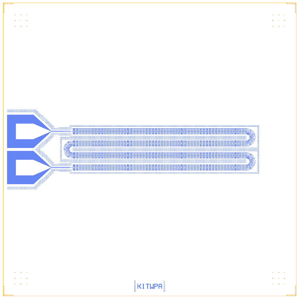
A kinetic-inductance travelling-wave parametric amplifier: a very long thin-film line whose inductance depends on the current. A DC bias and a pump give three-wave mixing along the line, and periodic loaded cells open a stop band that blocks the pump’s third harmonic. The geometry is the NY CREATES layout as ported in twpa-sim (MIT), redrawn as a negative mask on the Quantcore PDK.
This chip is dominated by one huge component: a 16-row serpentine of about 50 000 cells with two launches, two pads and two short feeds. The PDK Nb film is far less nonlinear than the source’s NbN.
At a glance
Notebook |
|
Source |
twpa-sim |
Chip |
7.5 × 7.5 mm Quantcore die (the source’s is 5 × 5 mm), sapphire 650 µm |
On the chip |
1 |
Builds today |
yes (layout built on 2026-11-19 in 15 s) |
How the notebook builds it
The amplifier notebooks use six Design segments (die, pads, feed, nonlinear element, routing, whole chip); see the notebook template.
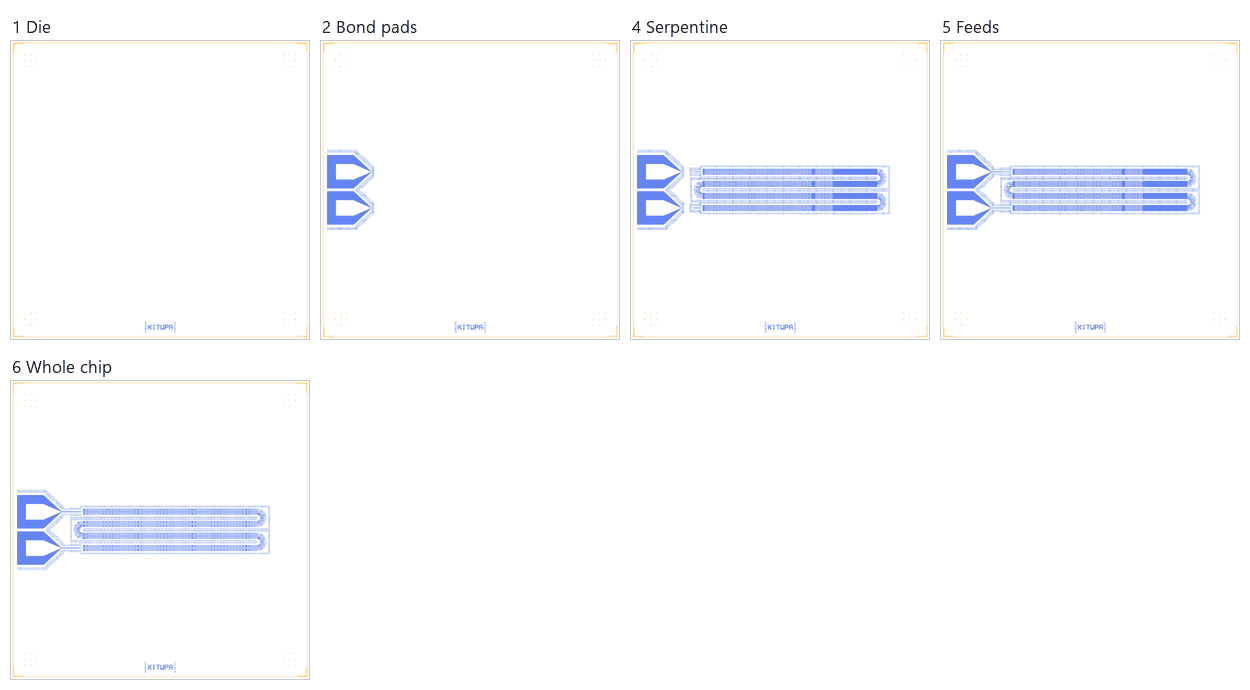
Die. The empty die with the QCT frame and the device ID
KITWPA.Bond pads. Input and output pads on the west edge, at the heights of the first and last rows.
Feed lines. No cell: signal, pump and DC bias share the serpentine’s own line; the feeds are drawn in segment 5.
Nonlinear element. The serpentine: rows of one supercell etch, radial U-turns, and the two launches.
Routing. Two short 50 Ω feeds from the pads to the launches.
Whole chip. The
launchsim group around the serpentine and the saved design.
LOM estimates
Numbers are from a run of this notebook on 2026-11-19 (Setup, Design, Check and the LOM cells, 16 s). This is an amplifier, so the LOM section gives gain and phase matching, not qubit frequencies. The line’s dispersion gives a stop band, and the 3WM coupled-mode gain is read at the pump:
line |
pump (GHz) |
G at f_p/2 (dB) |
max G (dB) |
|---|---|---|---|
PDK Nb |
no stop band below 12 GHz |
- |
- |
NbN 20 pH/□ |
8.985 |
14.8 |
14.8 |
twpa-sim v2 |
9.113 |
15.1 |
15.1 |
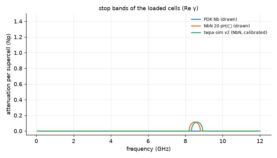
These are lumped-model estimates (component formulas and calibration), not FEM results. The LOM page says how far to trust them.
Build spec
The rest of this page is the detailed spec the notebook was built from, with every component, port, route and length.
Source · licence: mandalsoumyajit/twpa-sim (MIT): src/twpa/layout/kit.py, KITLayout, process kit_nycreates_research.json (NbN 20 pH/□). Die: 7.5 × 7.5 mm PDK die, PDK frame, sapphire 650 µm, Nb trilayer junctions. Notebook and design: examples/designs/amplifiers/ki_twpa_serpentine.ipynb / .json.
Components
instance |
catalog ref |
key params |
notes |
|---|---|---|---|
P_IN, P_OUT |
|
west edge (rows 0 and 15) |
|
KIT |
|
16 rows × 55 supercells (24 + 6 + 24 cells, 1.5 µm pitch), turns r 154 µm, 3 supercells per turn: 49 950 cells |
Routes
route |
from → to |
type |
|---|---|---|
L_IN |
P_IN.a → KIT.a |
CPW |
L_OUT |
P_OUT.a → KIT.b |
CPW |
LOM node structure
one conductor (wire between the pads); ladder from qcc_ladder (L_geo + L_s·squares, C per cell)
Targets (from the source)
twpa-sim v2: L 53.8 pH, C 22.3 / 8.4 fF per cell, ≈ 50 Ω, 3WM with DC bias
Simplifications / PDK differences
PDK Nb film (0.116 pH/□): ≈ 6 Ω, weakly nonlinear; NbN shown by a KineticInductance override in the analysis only