Filled qubit test chip (QPDK)
The qubit test chip from gdsfactory’s quantum-rf-pdk (QPDK), with a vortex-trap fill added to the ground plane: four double-pad transmons, each read out through its own λ/2 line hanging on a U-shaped probeline. The layout comes from QPDK’s filled_test_chip.py (MIT) and is rebuilt on the Quantcore PDK: sapphire, Quantcore junctions and the QCT die frame. The rebuild is distributed under GPL-3.0.
This notebook shows how a design is loaded read-only from another one, and how a foreign fill pattern becomes a PDK cheese rule (the original fill wins over the PDK band).
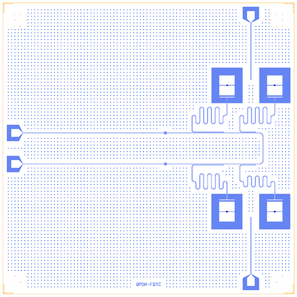
At a glance
Notebook |
|
Source |
gdsfactory |
Chip |
7.5 × 7.5 mm Quantcore die, the source’s 4250 × 6200 µm circuit centred in it, CPW 10 / 6 µm |
On the chip |
4 launchers · 4 double-pad transmons with trilayer SQUIDs · 4 λ/2 readouts · 1 probeline with 2 series IDCs · 2 flux lines · vortex-trap fill |
Builds today |
yes (layout built on 2026-11-19 in 5 s) |
How the notebook builds it
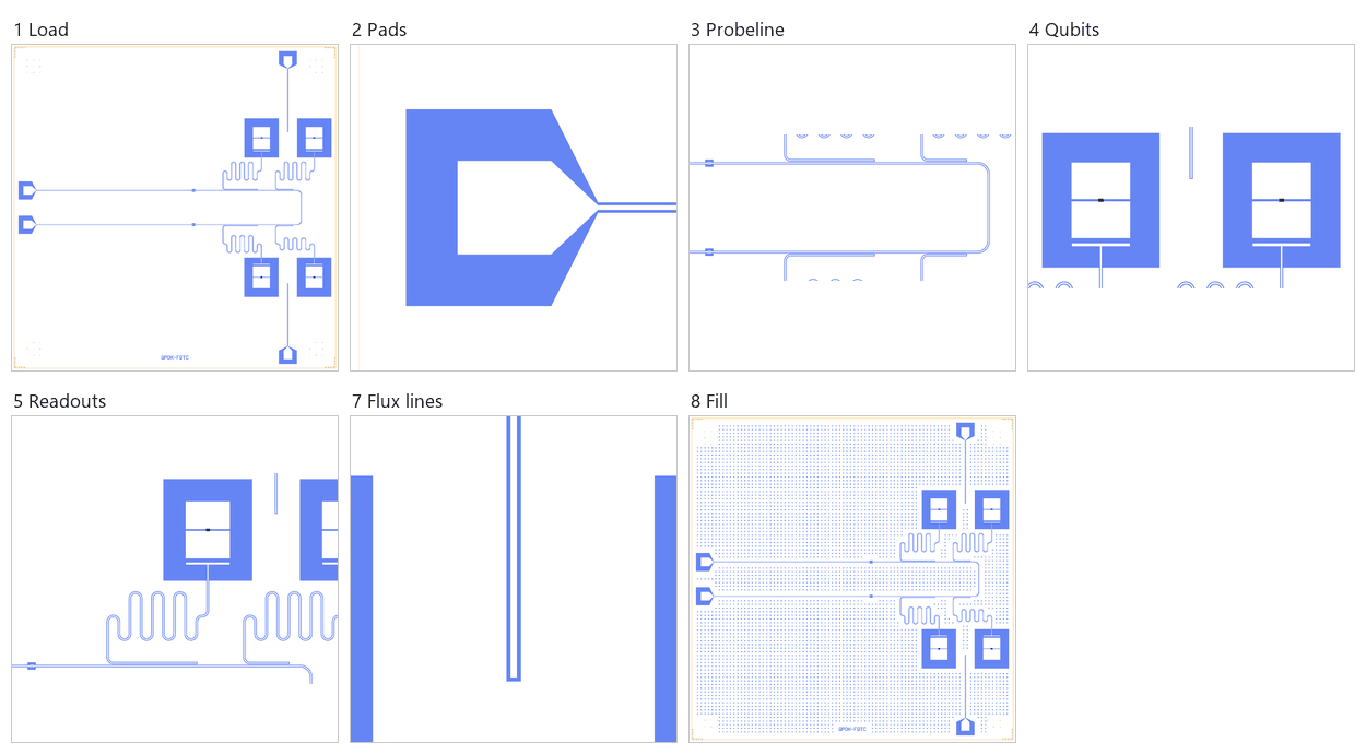
Load. The qubit test chip’s saved design is loaded read-only; only the name, the device ID and the cheese mode change.
Pads. The four launchers, 100 µm from the die edge (zoomed on the input pad).
Probeline. The two series IDCs and the U-shaped probeline between them.
Qubits. The double-pad transmons Q1 and Q2 with their SQUIDs (Q3 and Q4 mirror them).
Readouts. The λ/2 readouts that end in a coupled section on the probeline.
Coupling. None: the qubits only talk to their own readouts.
Flux lines. The open end of a flux line between two qubits, and the nine route lengths.
Fill. QPDK’s 15 µm vortex holes on an 85 µm pitch, written as the chip’s
cheeserule; the design is saved.
LOM estimates
Numbers are from a run of this notebook on 2026-11-19 (Setup, Design, Check and the LOM cells, 7 s): QuCat normal modes with QuTiP dressed values.
group |
qubit |
f_q (GHz) |
α (MHz) |
resonator |
f_r (GHz) |
κ (MHz) |
χ (MHz) |
|---|---|---|---|---|---|---|---|
Q1R1 |
Q1 |
5.763 |
-196 |
R1 |
11.87 |
0.638 |
-1.36 |
Q2R2 |
Q2 |
5.763 |
-197 |
R2 |
12.86 |
0.206 |
-1.27 |
Q3R3 |
Q3 |
5.764 |
-197 |
R3 |
16.16 |
0.4 |
1.61 |
Q4R4 |
Q4 |
5.763 |
-197 |
R4 |
12.33 |
0.713 |
-1.31 |
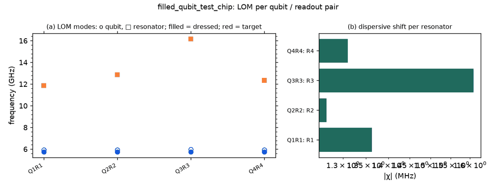
These are lumped-model estimates (component formulas and calibration), not FEM results. The LOM page says how far to trust them.
Build spec
The rest of this page is the detailed spec the notebook was built from, with every component, port, route and length.
Source: qpdk/samples/filled_test_chip.py
(filled_qubit_test_chip) · licence MIT (gdsfactory 2024, verified) · Read on 2026-11-02.
What it is: the qubit_test_chip YAML loaded unchanged. A vortex-trapping hole fill is added to
the ground plane, then a 100 µm etched chip-edge frame, and the result is converted to a negative (apply_additive_metals).
The sample says it “roughly corresponds” to Tuokkola et al., Methods to achieve near-millisecond coherence times in
superconducting quantum circuits (Nat. Commun. 2025). That paper’s fab GDS is the Zenodo record noted in
community/tuokkola_near_ms_transmon. Image: docs/_static/images/filled_qubit_test_chip.png.
Frame: chip_edge(size=(xsize + 230, ysize + 200), width=100) at (xmin − 100, ymin − 100) gives
box (0, 0, 4245, 6200) (the spec uses 4250). Designer = source + (100, 3100), the same frame as qubit_test_chip.
The components are the same as in qubit_test_chip; the fill is written as the chip’s cheese rule.
The same file also defines filled_flipmon_test_chip and filled_gatemon_test_chip (same fill on those YAMLs). For a
flip-chip YAML it also adds an M2 edge and an M2 fill (80 µm keep-out).
Components
Identical to qubit_test_chip → Components: PAD_IN, PAD_OUT, PAD_FT, PAD_FB,
C_IN, C_OUT, Q1–Q4 (DoublePads), same positions in the same Designer frame.
instance |
catalog ref |
key params (units) |
at (x, y) |
rot |
notes |
|---|---|---|---|---|---|
(chip) |
|
KQC ground grid |
box (0, 0, 4250, 6200) |
— |
stands in for |
EDGE |
chip frame |
100 µm etched border |
box edge |
— |
QPDK |
QPDK fill: 15 × 15 µm etched squares on a 70 µm gap grid, every second row staggered. The fill routine’s default keep-out keeps the squares clear of all drawn metal and etch. The rebuild matches it: hole 15 µm, pitch 85 µm, staggered rows.
Routes
Identical to qubit_test_chip → Routes (FL_IN, FL, FL_OUT, R1–R4 hangers, FLUX_T, FLUX_B).
Launchers, pads, test structures, markers, labels
4 launchers, chip edge, ground fill. No markers or labels.
LOM node structure
Same as qubit_test_chip. The fill does not change the netlist. It only lowers ground-plane capacitance slightly, so run FEM extraction on the filled geometry.
Targets
None stated. The reference device (Tuokkola 2025) is a single fixed-frequency transmon chip; this sample keeps the 4-qubit QPDK layout and borrows only the fill and edge treatment.
Simplifications for a first rebuild
Build qubit_test_chip first, then switch on
chip={"with_grid": True}.The exact QPDK fill geometry (15 µm squares, 70 µm gaps, stagger 2) is optional. The KQC grid is close enough for layout review; use the exact fill for FEM loss studies.
Build
The notebook examples/designs/qpdk/filled_qubit_test_chip.ipynb loads qubit_test_chip.json read-only. The fill is the chip’s cheese rule with QPDK’s 15 µm holes and 70 µm gap (the saved design has no KQC ground grid).
Quantcore PDK rebuild
The notebook is a Quantcore PDK rebuild, not a replica: the netlist, LOM and imported components are kept, the process is Quantcore’s.
Notebook: examples/designs/qpdk/filled_qubit_test_chip.ipynb.
Chip: the Quantcore die frame (L dicing markers 1000/0, 3 × 3 alignment grids 1001/0, chip boundary 100/0, device ID where an edge is free; any brand text is QCT), on the 7.5 × 7.5 mm Quantcore die; the source’s 4.25 × 6.2 mm chip area is centred in it (the box comes with the loaded qubit test chip), so every coordinate stays the source’s. The Quantcore frame replaces QPDK’s 100 µm etched
chip_edge.Stack: sapphire 650 µm, εr 10.25 (the PDK default stack, used by the LOM estimates and every FEM export); QPDK’s process is Al on Si (εr 11.45), so frequencies are not the QPDK ones.
Junctions: as in the qubit test chip (loaded with it): Quantcore trilayer SQUIDs on the PDK rule (
_qpdk.JJ_PARAMS): two 0.25 × 0.6 µm junctions (KQC’sjunction_width= the straight finger) → R_n 45 kΩ in parallel, L_J 6.73 nH at zero flux, C_J 15 fF; fingers on 2/0 + 4/0, spacer 50/0 with the 51–53/0 gradient (Nb Δ = 1.4 meV, R_n·A 13.5 kΩ·µm² and C_J 50 fF/µm² assumed).Kept: the topology and every component with the source’s parameters and positions, the readout / resonator lengths and coupled sections, the sim groups (the whole qubit test chip, loaded from its JSON).