One-qubit template (SQChip-EM)
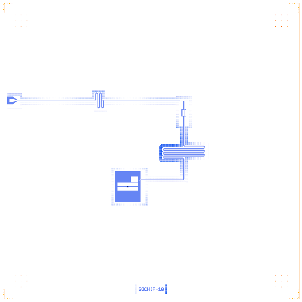
The one-qubit template of the SQChip-EM layout-to-EM dataset: a pocket transmon, an interdigital tee and a λ/2 readout feed to one launchpad. The repository states no licence, so treat the page as a reference; the notebook is a Quantcore PDK rebuild (GPL-3.0) of the Qiskit Metal generator metal_KDD_1qubit.py.
This notebook is an example of the smallest readout chain (qubit, tee, feed, pad) and of the order PDK placement needs: centre the core first, then the pad.
At a glance
Notebook |
|
Source |
|
Chip |
7.5 × 7.5 mm Quantcore die |
On the chip |
1 launchpad · 1 pocket transmon (L_J 12 nH) · 1 interdigital tee · 1 λ/2 readout · 1 feed line |
Builds today |
yes (layout built on 2026-11-19 in 7 s) |
How the notebook builds it
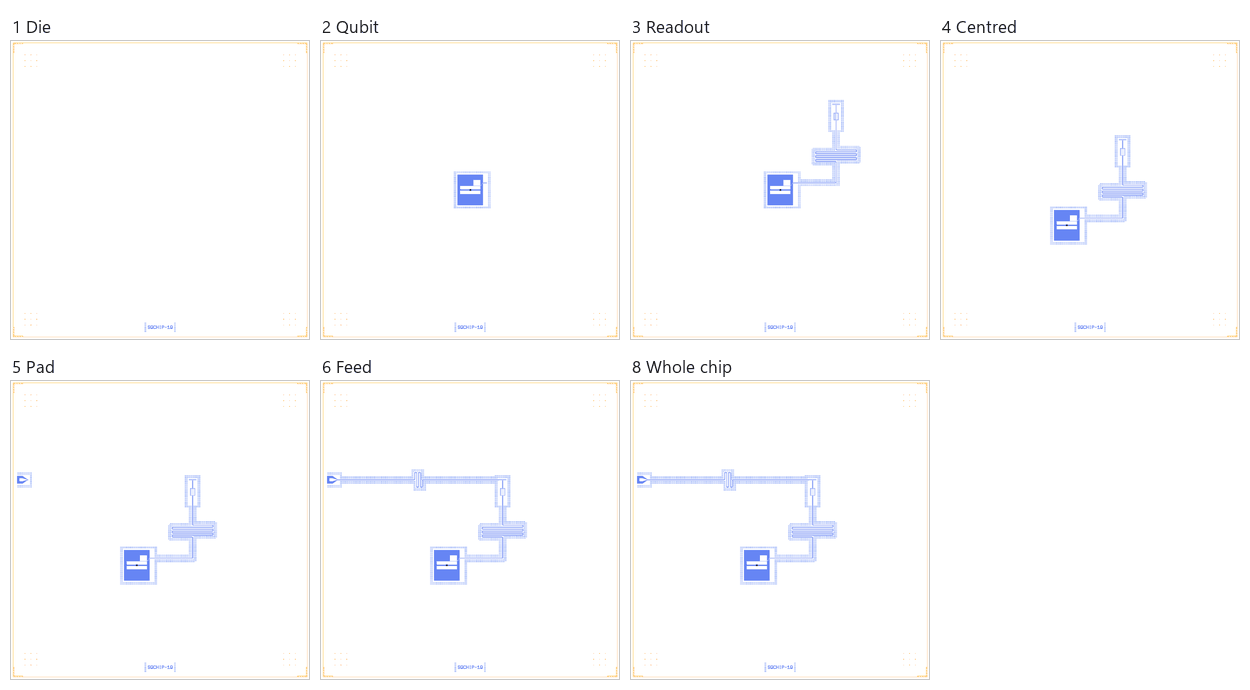
Die. The 7.5 mm die with the frame and the device ID
SQCHIP-1Q.Qubit. The pocket transmon with a trilayer junction (L_J 12 nH).
Readout. The interdigital tee and the λ/2 readout.
Centre. The core is centred in the die before the pad is placed.
Bond pad. The launchpad at the 100 µm pad rule.
Feed. The 5.5 mm feed meander from the pad to the tee.
Coupling and control. None: one qubit, no drive or flux line.
Whole chip. One sim group, targets, save.
LOM estimates
Numbers are from a run of this notebook on 2026-11-19 (Setup, Design, Check and the LOM cells, 8 s): QuCat normal modes with QuTiP dressed values.
mode |
kind |
f (GHz) |
κ (MHz) |
A (MHz) |
participation |
|---|---|---|---|---|---|
Q1 |
qubit |
5.396 |
1.52 |
252 |
J_Q1 0.97, RO_RES 0.03 |
RO_RES |
resonator |
6.131 |
93.4 |
0.3 |
RO_RES 0.97, J_Q1 0.03 |
group |
qubit |
f_q (GHz) |
α (MHz) |
resonator |
f_r (GHz) |
κ (MHz) |
χ (MHz) |
|---|---|---|---|---|---|---|---|
Q1R |
Q1 |
5.118 |
-301 |
RO_RES |
6.125 |
93.4 |
-8.37 |
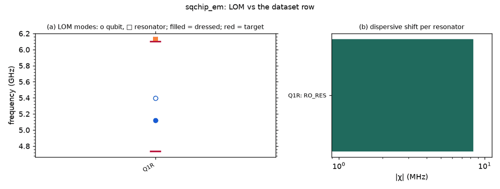
These are lumped-model estimates (component formulas and calibration), not FEM results. The LOM page says how far to trust them.
Build spec
The rest of this page is the detailed spec the notebook was built from, with every component, port, route and length.
The notebook
examples/designs/community/sqchip_em.ipynb(with its.jsonand PNGs) is the 1-qubit template as a Quantcore PDK rebuild, distributed under GPL.
The metal: references in this spec build as written, through the metal: wrapper (ports are the Metal pin names, parameters the Metal options); the Quantcore and KQC substitutions are optional.
Source: Secbrain/SQChip-EM (dataset DOI 10.5281/zenodo.20489133, per the
README badge). Licence: not stated. There is no LICENSE file and no licence section in the README, so treat it as
all rights reserved and use for reference only. Read on 2026-11-02: README, chip_code/metal_KDD_1qubit.py
(LayoutParams, populate_design), data/sqchip_em_{1q,2q}/summary.csv. The 3342 JSON/GDS records and the 3–8
qubit generators (1.2k–5.8k lines each) were not read in detail.
What it is: an ML benchmark linking parameterised Metal layouts to HFSS eigenmode (pyEPR) and Q3D LOM results.
Public data covers 1-qubit (532 rows) and 2-qubit (35 rows) splits. The 3/4/6/8q folders are empty placeholders.
README renders exist for 2, 3, 4, 5, 6, 8-qubit chips (figure/final_*q_ro_res_bus.png).
The chip uses metal:TransmonPocket and metal:CapNInterdigitalTee. The source is a reference only.
1-qubit template (metal_KDD_1qubit.py)
Frame: chip 12 × 12 mm centred. Designer = source + (6000, 6000). CPW 10/6.
instance |
catalog ref |
key params (units) |
at (source, mm) |
notes |
|---|---|---|---|---|
Q1 |
|
pad_width 520, pocket_height 780. Readout pad (loc_W +1, loc_H +1) 180 × 150, gap 1.4 µm (sweep default) |
(dx, dy), swept −10…+10 mm (24 values each) |
|
RO_TEE |
|
prime 14/6, second 10/6, finger_count 12, finger_length 160, cap_gap 1.2, cap_width 8, cap_distance 220 |
readout pin + (1.0, 2.0) mm |
readout resonator couples to the feedline through an interdigital tee |
LP_RO |
|
tee − (2.4, 0) mm |
||
RO_FEED |
route LP_RO.tie → RO_TEE.prime_start |
meander 5.5 mm, spacing 280, leads 250/250, fillet 25 |
feedline (one launcher; prime_end is not routed) |
|
RO_RES |
route RO_TEE.second_end → Q1.readout |
meander 8.5 mm (ro_L), spacing 260, leads 250/250 |
capacitive at both ends (λ/2 type) |
1q dataset values: Lj 12 nH, Cj 2 fF. f_q 4.60–4.83 GHz, f_r 5.73–6.26 GHz, g/2π 200–294 MHz, χ 4.7–7.8 MHz, κ/2π 5.3–6.1 MHz, C_in ≈ 52 fF. Only the qubit position varies across the 532 rows.
2-qubit split (summary only)
Q1 at (−1.5…0, 0…1.5) mm, Q2 at (0…2, −1.5…2) mm. Lj 3 or 12 nH, ro_L 8.5–9 mm, the same tee. Readouts, a bus
and a resonator per qubit (render final_2q_ro_res_bus.png). Many rows are unphysical (f_q 1.7–22.6 GHz,
g up to 8.4 GHz), so filter on status.
LOM node structure
1q: floating pocket transmon (2 pad nodes + JJ) → readout pad C_g → RO_RES (λ/2, 8.5 mm) → interdigital C_in ≈ 52 fF →
feedline → one 50 Ω port. N-qubit: same per qubit, plus buses (ro_res_bus renders).
Simplifications for a first rebuild
The 1q record serves as a LOM cross-check rather than a rebuild target: our
DoublePads+ λ/2 route + finger capacitor should land near f_r ≈ 6 GHz and g ≈ 0.2–0.3 GHz for Lj 12 nH.
Rebuild (Quantcore PDK)
Frame and stack: the PDK 7.5 mm die (device ID
SQCHIP-1Q; the source’s 12 mm canvas is mostly empty) and the PDK stack (sapphire).Cells:
metal:TransmonPocket(pads 520 µm, pocket height 780 µm, readout pad 180 × 150 µm, gap 1.4 µm) andmetal:CapNInterdigitalTee(prime 14/6, second 10/6, 12 fingers × 160 µm, gap 1.2, cap distance 220), at the source’s offsets: tee = readout pin + (1.0, 2.0) mm, launchpad = tee − (2.4, 0) mm.Routes: qcc meanders of the source’s lengths, 5.5 mm feed and 8.5 mm λ/2 readout. The tee’s
prime_endis left open, as in the source.Junction:
Quantcore Junctionat the dataset’s L_J = 12 nH (registry.trilayer_junction(..., lj_nH=12)).Quick check (script run of the cells, not nbclient):
DRC: 0 errors, 3
dangling_port(squid_a/b, the openprime_end);LOM: 4 nodes;
LOM sim: f_q 5.12 GHz against the dataset’s 4.734 (the LOM C_Σ is lower than HFSS); f_r 6.22 GHz against 6.099 (sapphire vs Si); χ −7.35 MHz against 4.7–7.8; κ 94.5 MHz against 5.3–6.1.
κ is far too large: the LOM’s IDC estimate for 12 × 160 µm fingers at a 1.2 µm gap gives C_in well above the dataset’s ≈ 52 fF (a limit of the LOM’s IDC model).
FEM: the q3d and eigenmode jobs
Q1Rhave netsQ1.island1/2.