Lumped JPAs, two couplings
The simplest Josephson parametric amplifier: one junction shunted by a capacitor, a lumped LC mode pumped near resonance. The chip has two of them, one coupled to its line through a series capacitor and one through a shared (tapped) inductance. The layout follows twpa-sim’s jpa families (MIT) on the Quantcore PDK.
This notebook compares two ways of coupling a lumped mode to a 50 Ω line, side by side on one die, each with its own pad.
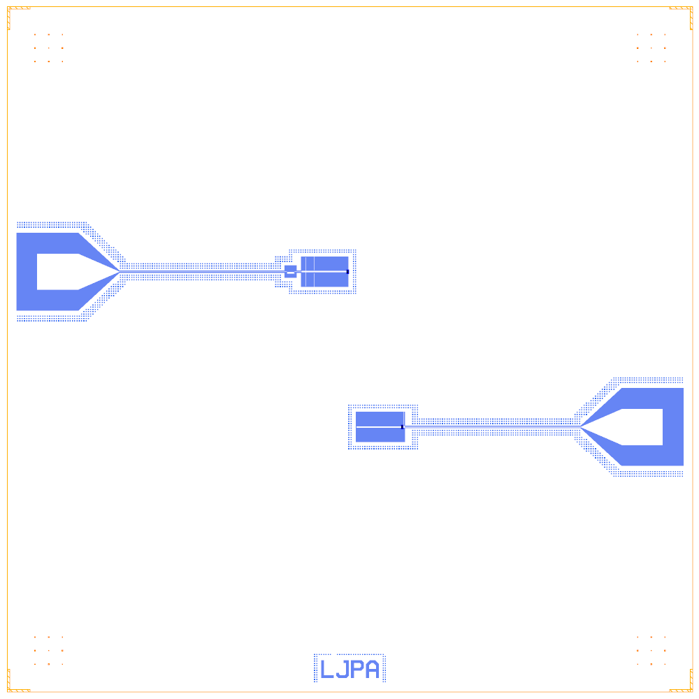
At a glance
Notebook |
|
Source |
twpa-sim |
Chip |
7.5 × 7.5 mm Quantcore die, sapphire 650 µm |
On the chip |
2 |
Builds today |
yes (layout built on 2026-11-19 in 5 s) |
How the notebook builds it
The amplifier notebooks use six Design segments (die, pads, feed, nonlinear element, routing, whole chip); see the notebook template.
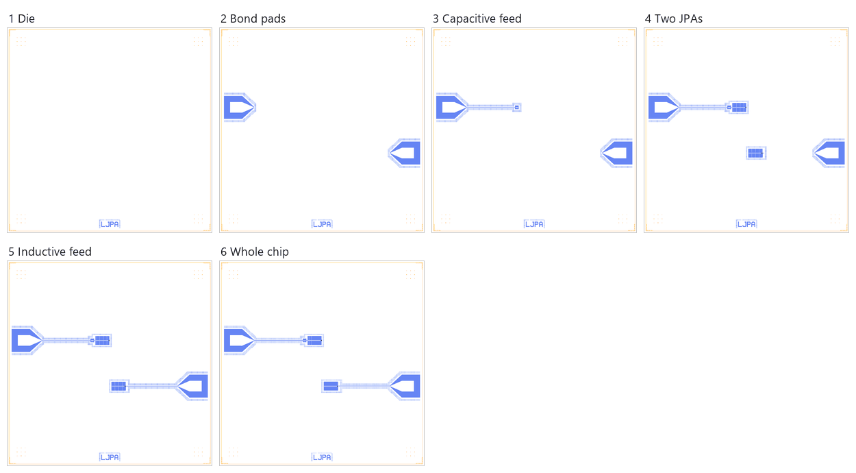
Die. The empty die with the QCT frame and the device ID
LJPA.Bond pads. One pad per JPA: the capacitive one from the west edge, the inductive one from the east edge.
Capacitive feed. The finger coupling capacitor (12 fingers × 80 µm) and its 50 Ω line.
Nonlinear elements. The two lumped JPAs, with the junction sized to the PDK limit and tabulated against the source.
Routing. The inductive JPA’s feed, ending on its tap strip.
Whole chip. The two sim groups (
jpa_c,jpa_l) and the saved design.
LOM estimates
Numbers are from a run of this notebook on 2026-11-19 (Setup, Design, Check and the LOM cells, 7 s). This is an amplifier, so the LOM section gives gain and phase matching, not qubit frequencies. The chip carries two JPAs, a capacitive and an inductive one:
JPA |
f0 (GHz) |
κ/2π (MHz) |
Q_ext |
K/2π (MHz) |
|---|---|---|---|---|
capacitive |
6.592 |
40.4 |
163 |
16.8 |
inductive |
6.802 |
95.8 |
71 |
17.9 |
The single-mode Kerr model (undepleted pump) gives a peak gain of 20.4 dB at -123.6 dBm.
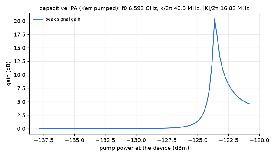
These are lumped-model estimates (component formulas and calibration), not FEM results. The LOM page says how far to trust them.
Build spec
The rest of this page is the detailed spec the notebook was built from, with every component, port, route and length.
Source · licence: mandalsoumyajit/twpa-sim (MIT): src/twpa/layout/generate.py (families jpa, inductive_coupler), examples/layout/jpa*.json. Die: 7.5 × 7.5 mm PDK die, PDK frame, sapphire 650 µm, Nb trilayer junctions. Notebook and design: examples/designs/amplifiers/twpa_sim_jpa.ipynb / .json.
Components
instance |
catalog ref |
key params |
notes |
|---|---|---|---|
P_C, P_L |
|
west / east edge |
|
CC |
|
12 fingers × 80 µm |
|
JC |
|
capacitive, snapped to CC.b; 30 fingers/side × 150 µm IDC; PDK max junction |
|
JL |
|
inductive (tap strip 8 µm), rot 180; same IDC and junction |
Routes
route |
from → to |
type |
|---|---|---|
L_C |
P_C.a → CC.a |
CPW |
L_L |
P_L.a → JL.signal |
CPW |
LOM node structure
JC: island (C_shunt, JJ to ground), then C_c π, then pad; JL: island (C_shunt), then JJ, then tap (L_tap + C_tap to ground, pad)
Targets (from the source)
none stated (illustrative process: f0 ≈ 63 GHz)
Simplifications / PDK differences
planar IDC instead of MIM; PDK junction (0.65 µA) instead of 20 µA; galvanic tapped inductance instead of a pickup loop; junctions are flagged pdk_rn where present (amplifier junctions are far below the qubit R_n window).