Qartographer wire routing
Qartographer (MIT, © 2025 Adyoth Sural) is an optimiser that places drive and readout wire paths from fixed perimeter points to the qubits of a device map, penalising wires that run too close together or too long. Its shipped example is a 7 × 7 grid of 49 qubits with one optimised drive path per qubit, given as JSON. The notebook rebuilds that example on the Quantcore PDK (GPL-3.0) as a wiring demonstrator: 49 Xmons on the optimiser’s grid, 49 bond pads where its drive points are, and one drive line per path.
This notebook is an example of a chip built from an external tool’s coordinates: one scale for the whole map, pads on the PDK edge rule in the tool’s order, and lines that pass between the same qubits as the tool’s straight paths without cutting through any cross.
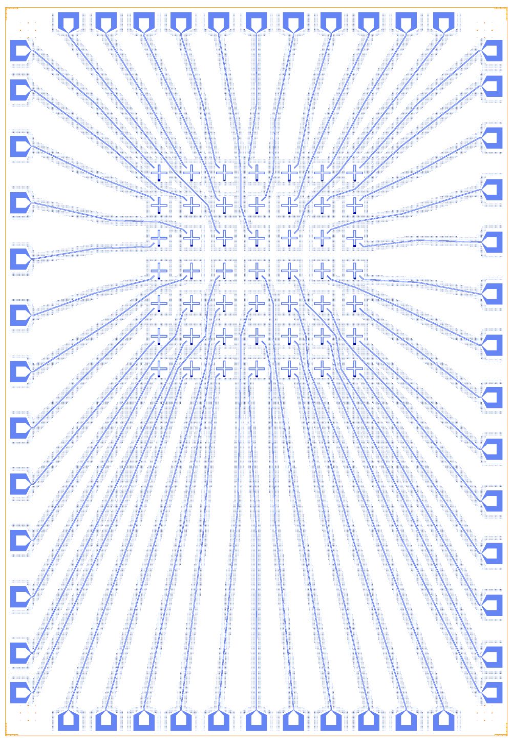
At a glance
Notebook |
|
Source |
|
Chip |
10 × 14.5 mm Quantcore die; the map scaled by 11.21 (650 µm qubit pitch); CPW 10 / 6 µm |
On the chip |
49 bond pads · 49 Xmons (KQC |
Builds today |
yes (layout built on 2026-11-19 in 15 s) |
How the notebook builds it
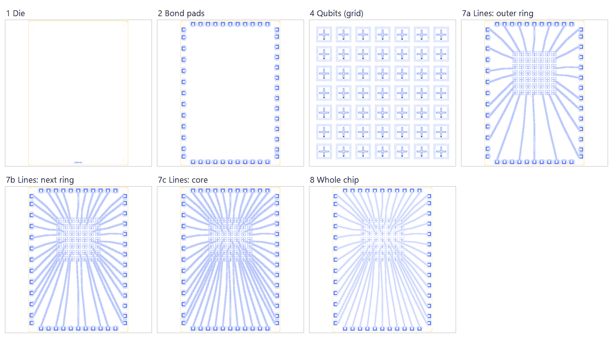
Die. The 10 × 14.5 mm die with the frame. The device ID fits on the empty die but not once the pads fill every edge, so the finished chip has none.
Bond pads. 49
BondPads (200 µm pads) on the 100 µm pad rule, each at its drive point’s place along the edge; the four corner points move onto the left and right edges, 860 µm from the corners.Readout line. None: the data’s multiplexer line ends inside the grid and its readout paths cross the drive paths 80 times.
Qubits. 49
Swissmoncrosses on the 650 µm grid, each with its drive end in the quadrant its drive path leaves in.Readout resonators. None in the source.
Coupling. None drawn: the 84 neighbour pairs carry no coupler geometry, and the gaps between neighbours carry the drive lines.
Drive lines. Three batches: the outer ring (24 lines straight out), the next ring (16), the core (9).
Whole chip. Two sim groups, the centring check (no shift), save.
Inside the grid each line passes through the same gaps between neighbouring qubits as the optimiser’s straight path, at the middle of the gap (two lines in one gap sit 50 µm either side of it). Outside the grid it runs through the optimiser’s middle point to its pad.
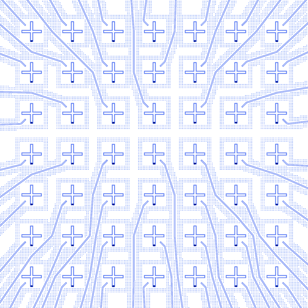
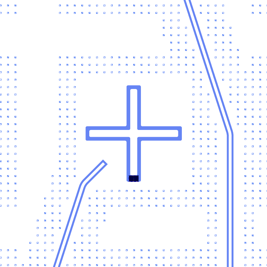
The second zoom is Q17: its own line ends open 100 µm off both arm axes in the lower-left quadrant, and Q24’s line passes on its right.
LOM estimates
Numbers are from a run of this notebook on 2026-11-19 (Setup, Design, Check and the LOM cells, 50 s): QuCat normal modes with QuTiP dressed values. Each qubit with its drive line and pad is one group, and all 49 groups give the same values.
groups |
f_q (GHz) |
α (MHz) |
QuCat mode (GHz) |
κ through the drive line (kHz) |
T1 limit (µs) |
|---|---|---|---|---|---|
Q0 … Q48, each with its drive line and pad (49) |
6.128 |
-225.1 |
6.343 |
1.35 |
118 |
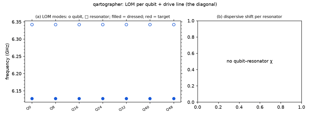
The LOM can estimate each qubit’s frequency and anharmonicity and the T1 limit its own drive line sets through the pad’s 50 Ω port. That limit comes from the library’s rough 0.1 fF drive capacitance, and a drive line is one node in the LOM, so its length and path do not enter. The LOM cannot estimate the wiring itself: the capacitance between a qubit and the neighbours’ lines that pass it (the Q17_passing Q3D job measures it), coupling between lines, or the real drive capacitance (the Q24_drive Q3D job). Shortening Q24’s arms from 150 to 130 µm raises f_q to 6.505 GHz and |α| to 256 MHz (LOM 3).
These are lumped-model estimates (component formulas and calibration), not FEM results. The LOM page says how far to trust them.
Build spec
The rest of this page is the spec the notebook was built from: the source data and how the rebuild maps it onto the die.
Source: AYDOSUL/Qartographer (A. Sural) · licence MIT (“Copyright (c) 2025
Adyoth Sural”, checked in LICENSE). The README, INFO.md and Documentation/JSONguide.md describe the tool; the
notebook takes its numbers from Documentation/7x7 Qubit Placement.json and Documentation/7x7 Wiring Data.json
(read on 2026-11-19). The optimiser (Code/Qartographer.py, SciPy) was not run.
What it is: a cost-function optimiser that places control and readout wire paths from fixed perimeter “drive points”
to qubits, penalising short spacing and long length. JSON in and out (qubit placement, wiring data, merged device map).
The repository has data for the 7 × 7 (49-qubit) example only.
Data: coordinates in metres. Qubits are on a 58 µm pitch (x 677…1025 µm, y −95…253 µm), so this is an abstract
map, not a fab layout. optimized_couplings lists the 84 nearest-neighbour pairs. The 49 fixed drive points sit on an
800 × 1200 µm rectangle (x 450…1250 µm, y −700…500 µm), four of them on its corners; optimized_drive_paths[k] runs
from Qubit_k through a middle point (on the straight line, at the mean of its ends) to fixed_drive_points[k]. No
two of these straight paths cross. The wiring file also has one multiplexer line, from (866.8, −38.1) to
(830.7, 194.4) µm, and a readout tap on it per qubit.
Components / routes
item |
content |
rebuild |
|---|---|---|
qubits |
Qubit_0…Qubit_48, 7 × 7, 58 µm pitch |
|
couplings |
nearest-neighbour pairs ( |
checked against the grid; not drawn |
wiring |
one optimised path per qubit from a fixed drive point |
|
drive points |
49 points on the rectangle’s sides and corners |
|
readout |
one multiplexer line, 49 taps |
not built |
LOM node structure
49 grounded transmons, each island with its capacitance and junction to ground and a drive control: the line’s conductor keeps its pad’s 50 Ω port and couples to the island through 0.1 fF (the library’s rough charge-line value). No couplers, resonators or feedline. The source’s lattice of 84 neighbour pairs has no coupler geometry.
Rebuild (Quantcore PDK)
Scale and die. One scale for the whole map, 650 / 58 ≈ 11.21, about the centre of the drive-point rectangle, which goes to the centre of a 10 × 14.5 mm die. The rectangle becomes 8.97 × 13.45 mm; the grid spans 3.9 mm and sits 2.0 mm above the die centre, as it sits above the rectangle’s centre in the map. Sapphire 650 µm, εr 10.25; the PDK band cheese (the source has none).
Pads. Each drive point’s pad goes on the die edge of its side of the rectangle, at the same place along it;
edge="auto"puts its etch 100 µm from the edge. The frame’s corner marker areas reach 600 µm from each edge, so the four corner points (Q5, Q23, Q42, Q48) get pads on the left and right edges, centred 860 µm from the corner. Edges: 11 pads at the bottom, 11 at the top, 13 on the left, 14 on the right.Lines. The straight path of an inner qubit passes as close as 5.4 µm (in the map) to another qubit’s centre, so the lines follow the gaps the paths pass through rather than the exact lines: each path that crosses the gap between two neighbours is put at the middle of that gap (at most two per gap, ± 50 µm), in the order the paths cross it. The waypoints from the pad: the optimiser’s middle point, the gap points, an approach point on the quadrant’s diagonal, then the drive end 100 µm off both arm axes. The 24 outer-ring qubits cross no gap. Bends are r = 50 µm. The planned centre lines are at least 89 µm apart; the lines are 2.5 to 9.2 mm long, 238 mm in all.
Not built. The couplings (no geometry, and every gap may carry a drive line) and the readout network: the 49 straight readout paths would cross the drive paths 80 times, and the multiplexer line ends inside the grid with no pad.
DRC: 0 errors; 147
dangling_portwarnings (each Swissmon’s three zero-length coupler ports); no PDK design warnings.FEM jobs:
Q24_drive(Q24 in a box 250 µm beyond its cross, cuttingD24; Q3D C-matrix and eigenmode) andQ17_passing(Q17’s box, which also cutsD24; Q3D C-matrix with netsQ17.island,D17,D24). They are exported, not solved.Feedback exercise. The source has no targets. The notebook detunes Q24 to 5.90 GHz with a first-order L_J rule on a design copy; one step (L_J 6.73 → 7.32 nH, R_n 48.9 kΩ) lands at 5.905 GHz in the LOM.