Transmon with readout (Metal A.1)
One pocket transmon with a meandered λ/4 readout resonator, hanging off a straight feedline between two bond pads through a coupled-line tee. It is the Qiskit Metal “A.1” full-design example (Apache-2.0, © IBM and contributors), which itself adapts the SQDMetal benchmark devices. The Quantcore rebuild is distributed under GPL-3.0.
Build this one first. It is the smallest complete qubit chip, with a qubit, a resonator coupled to a feedline and the
bond pads that carry the signal in and out. It shows how a Metal component is placed through the metal: wrapper and
how the PDK moves the bond pads to its 100 µm edge rule.
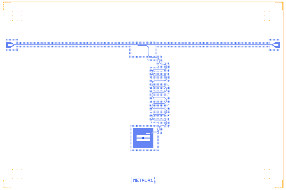
At a glance
Notebook |
|
Source |
Qiskit Metal |
Chip |
9 × 6 mm (the source’s size, larger than the 7.5 mm Quantcore die), CPW 10 / 6 µm |
On the chip |
1 pocket transmon · 1 λ/4 readout (7 mm) · 1 coupled-line tee · 1 feedline · 2 bond pads |
Builds today |
yes (layout built on 2026-11-19 in 8 s) |
How the notebook builds it
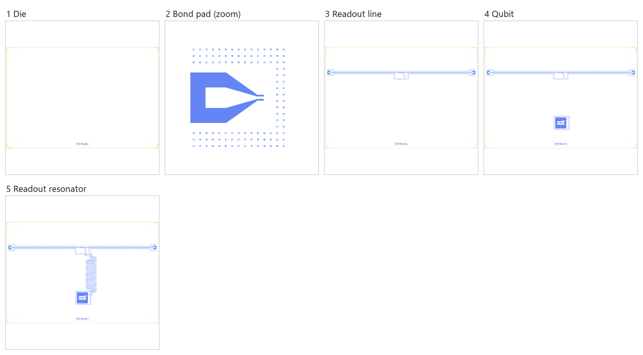
Die. An empty 9 × 6 mm chip with the QCT frame (dicing marks, alignment grids, chip boundary, device ID).
Bond pads. Two launchpads, slid to the 100 µm pad-edge rule (the picture zooms on one pad).
Readout line. The coupled-line tee on its feedline, 1.5 mm above the chip centre.
Qubit. One Metal pocket transmon with the Quantcore trilayer junction.
Readout resonator. A 7 mm λ/4 meander from the tee’s coupled arm to the qubit’s readout pad.
Coupling. Nothing to place: the only coupling is the readout pad to its resonator.
Control lines. None; the qubit is driven and read through its readout.
Whole chip. The sim group (qubit, readout and tee), the content centred in the die, the design saved.
LOM estimates
Numbers are from a run of this notebook on 2026-11-19 (Setup, Design, Check and the LOM cells, 9 s): QuCat normal modes with QuTiP dressed values.
mode |
kind |
f (GHz) |
κ (MHz) |
A (MHz) |
participation |
|---|---|---|---|---|---|
clt |
resonator |
3.931 |
0.0898 |
0 |
clt 1.00 |
Q1 |
qubit |
7.769 |
0.000599 |
311 |
J_Q1 1.00 |
parameter |
LOM (QuTiP) |
target |
|---|---|---|
|
3.93 |
– |
|
0.0898 |
– |
|
-0.205 |
– |
|
7.44 |
– |
|
-345 |
– |
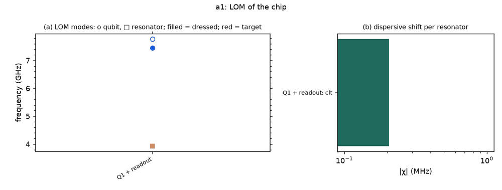
These are lumped-model estimates from component formulas and calibration, not FEM results. The LOM page says how far to trust them.
Build spec
The rest of this page is the detailed spec the notebook was built from: every component, port, route and length.
The
metal:references in this spec build as written, through themetal:wrapper (ports are the Metal pin names, parameters the Metal options). The Quantcore and KQC substitutions are optional.
Source: Quantum Metal docs/tut/full-design-examples/A.1-Transmon-with-readout-resonator.ipynb. Licence Apache-2.0.
It is adapted from the SQDMetal benchmark devices (Sommers et al., arXiv:2511.01220, 2025; Apache-2.0).
This is the canonical unit cell: a TransmonPocket with one readout pad, and a meandered λ/4 resonator hanging off a
straight feedline between two wire-bond pads through a CoupledLineTee (shorted at the tee).
Chip: DesignPlanar default 9000 × 6000 µm, centred, so Designer = Metal + (4500, 3000). CPW 10/6 µm, fillet 90
µm. Metal layer 1; no junction file.
A first build uses these substitutions: KQC DoublePads (or Xmon) for TransmonPocket, a hanger for CoupledLineTee,
and BondPad. This is the Metal twin of the Quantcore Q1/R1 example in the README.
Components
instance |
catalog ref |
key params (µm) |
at (x, y) |
rot |
notes |
|---|---|---|---|---|---|
Q1 |
KQC |
Metal pad_width 425, pad_height 90, pad_gap 30, pocket 650 × 650; readout pad (loc_W +1, loc_H +1) 125 × 30, pad_gap 15 |
(4500, 1500) |
0 |
DoublePads |
CLT |
hanger on FL (metal:CoupledLineTee) |
coupling_length 350, coupling_space 3 (default), down_length 300, fillet 90, open_termination False |
coupler centre (4500, 4500) |
0 |
leg at x + 175 (downstream), short at x − 175 |
LP1 |
|
Metal default pad, lead 25 |
(525, 4500) |
270 |
|
LP2 |
|
same |
(8475, 4500) |
90 |
faces W |
Routes
route |
from → to |
type, length |
waypoints / hanger |
notes |
|---|---|---|---|---|
FL |
LP1.a → LP2.a |
cpw 7950 |
— |
Metal feed_L + tee prime (700) + feed_R; straight at y = 4500 |
R1 |
Q1.cplr → |
meander 7650 |
— |
Metal total_length 7000 (tee second_end → qubit pin, leads 100/100) + 300 down leg + 350 coupled section |
Hanger check: second_end (4675, 4175) sits 325 µm below the feed (300 leg + 25 = 5 + 6 + 3 + 6 + 5), so ground_gap is 3.
Launchers, pads, test structures, markers, labels
2 pads (W/E). There are no markers, labels or test structures.
LOM node structure
Q1 is an island pair with a JJ and C_g to R1. R1 is λ/4, open at the qubit coupler and shorted at the hanger, with a coupled-line κ to FL. FL is a through line between two 50 Ω ports (LP1, LP2). There are no control lines.
Targets (if stated)
None in the notebook. total_length 7 mm sets the readout frequency: λ/4 ≈ 7.65 mm gives about 4.1 GHz on sapphire
(3.9 on Si), an estimate. Retune with d.targets(R1=...).
Simplifications for a first rebuild
Use DoublePads with the pocket’s pad sizes. The single centred coupler replaces the corner connection pad.
Use one straight FL route through the hanger. The CLT’s 90 µm fillet is not reproduced.
This is the simplest test of hanger κ and C_g estimates against the Metal reference.
Quantcore PDK rebuild
The notebook is a Quantcore PDK rebuild of the source, not a replica: the netlist, LOM and imported components are kept, and the process is Quantcore’s.
Notebook: examples/designs/metal/a1_transmon_readout.ipynb.
Chip: the Quantcore die frame (L dicing markers 1000/0, 3 × 3 alignment grids 1001/0, chip boundary 100/0, device ID where an edge is free; any brand text is QCT), drawn on the source’s 9 × 6 mm chip (the design does not fit the 7.5 mm die); no KQC chip frame.
Stack: sapphire 650 µm, εr 10.25 (the PDK default stack, used by the LOM estimates and every FEM export); Metal’s
DesignPlanardefault is silicon (εr 11.45, 750 µm), so the LOM capacitances, resonator frequencies and FEM jobs here are for sapphire rather than the source’s substrate.Junctions: Quantcore Nb/AlOx/Nb trilayer junctions (
junction_typefromlayouts.registry.trilayer_junction): fingers on 2/0 + 4/0, spacer 50/0 with the 51–53/0 gradient, sized on the PDK junction rule (Nb Δ = 1.4 meV, I_c·R_n = πΔ/2e, R_n·A 13.5 kΩ·µm² and C_J 50 fF/µm² assumed);Q1gets the PDK nominal junction, 0.5 × 0.6 µm fingers → R_n = 45 kΩ, L_J = 6.73 nH, C_J = 15 fF (in the 40–50 kΩ window), in place of Metal’shfss_inductance10 nH (+ 2 fF assumed). Expected f_q ≈ 7.4 GHz (an estimate from a LOM C_Σ of about 61 fF), still above the ≈ 4 GHz λ/4 readout as in the tutorial.Kept: the topology and every Metal component with the source’s options (through the
metal:wrapper), positions and orientations, every route’s end pins and total length, the sim groups (the 7 mm readout meander, the tee’s 350 µm coupling length, the feedline halves).