Quick prototype in KLayout
At the end you will have a chip with one Xmon qubit (Q1), one readout resonator (R1) on a feedline, and a flux line, drawn in KLayout. You will also have checked it, run the lumped-circuit (LOM) estimate, exported a simulation job and written the fab files.
Before you start
The Quantcore plugin is installed in KLayout. See the KLayout plugin for the install.
1. New design and chip
Open Quantcore > Design > New design… and save the file, for example as hand_q1r1.json. Leave Square die
ticked and keep the die width at 7500 µm. The empty die builds with its frame and label.
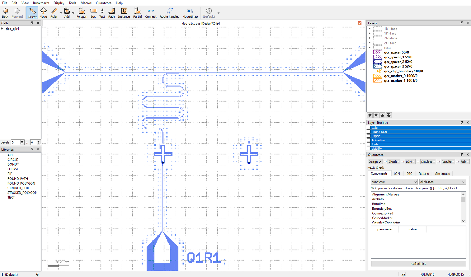
The Quantcore menu, the three toolbar tools and the Quantcore panel.
2. Place the qubit
In the Components tab, click Xmon. Set junction_type to Trilayer Squid and flux_port to true, then
double-click Xmon and click near (2975, 2200).
In Move/Snap, double-click the qubit and set x 2975 and y 2200. Set the targets f_q 5.1 GHz and α −220 MHz. In the same dialog, set the junction L_J to 12 nH. Without it the LOM has no qubit.
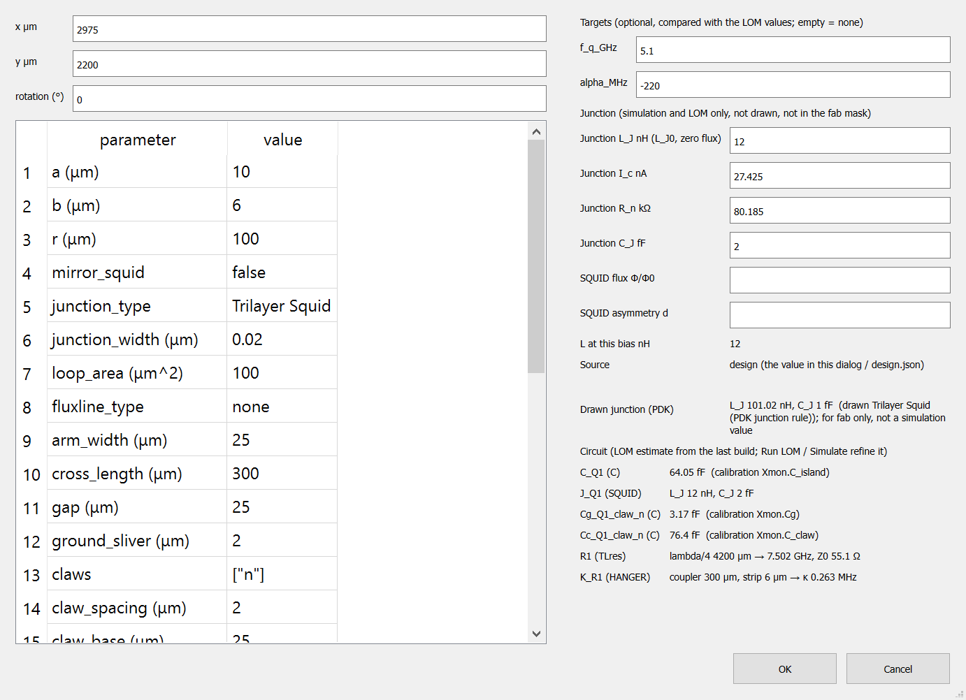
The component dialog of the Xmon: position, targets and junction.
3. Place the pads and feedline
Double-click BondPad in the Components tab and click near (1125, 3750). Turn it with [ or ] so that its
port arrow points into the chip. Place a second BondPad near (6375, 3750), turned the other way.
Place a third BondPad for the flux line near (2964.5, 750), facing up. In its table set pad_width 300, pad_height
300, pad_gap 150 and taper_length 300.
With Connect, click the port of the west pad, then the port of the east pad. In the route dialog, name the route
FL and set its type to cpw.
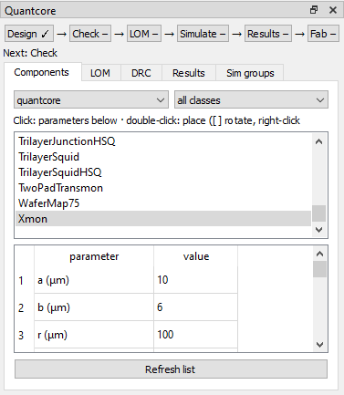
The Components tab. Pick the library and the class, then double-click a cell to place it.
4. Add the readout resonator
Hanging the resonator is the same as drawing a route. With Connect, click the qubit’s claw port Q1.claw_n, then
click on the feedline at about x 3125.
In the hanger dialog, leave Merge into FL (T-junction) unticked. Set the name R1, the type meander,
Meander length µm 4200, Coupler length 300, Side right and Ground strip 6. Press OK.
In Route handles, double-click R1 on a straight part. Set the targets f 7.2 GHz and g 90 MHz.
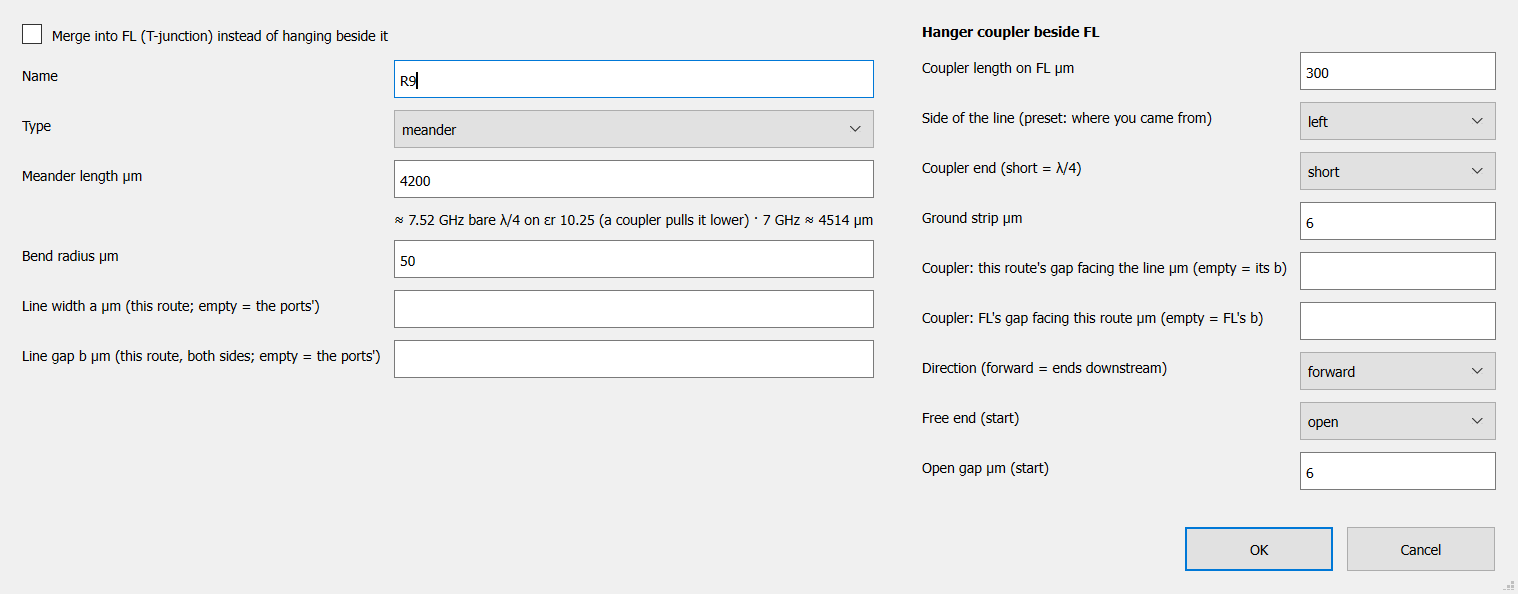
The hanger dialog: the readout resonator hangs off the feedline.
5. Route the flux line
With Connect, click the flux pad’s port. Hold Shift and click at about (2964.5, 1967), straight above the pad.
Then click the qubit’s flux port Q1.flux.
In the route dialog, name the route FLUX, set its type to cpw, Line width a 4 and Line gap b 6.
In Route handles you can drag any node to change the line. Double-click a node to set its exact position.
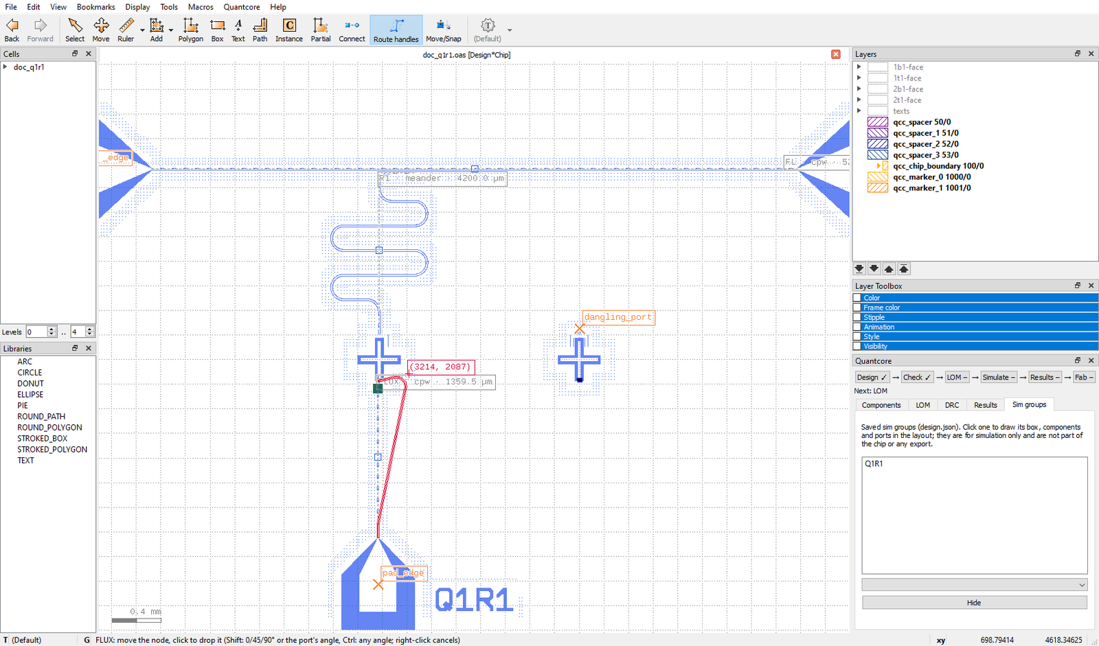
Route handles: click a node to pick it up and click again to drop it.
6. Check the design
Press Ctrl+Shift+D or click Check in the Flow strip. The DRC tab lists the errors, the warnings and the PDK design warnings. There should be no errors. Click a line to zoom to its marker.
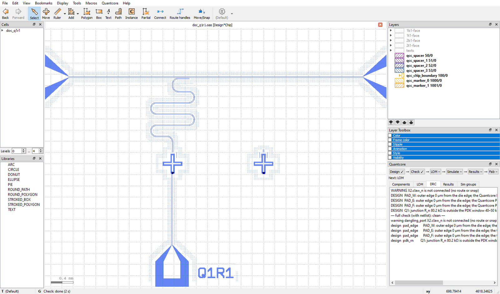
The DRC tab after Check. This picture is from another scratch design.
7. Run the LOM
Press Ctrl+Shift+O or click LOM in the Flow strip, then click Run LOM in the LOM tab. For Q1 + R1 the run takes a few seconds. f_q should land near 5.1 GHz and f_r near 7.2 GHz.
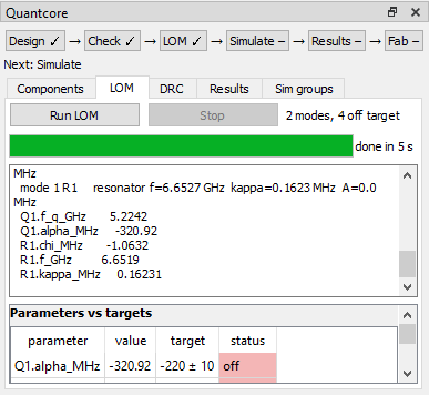
The LOM tab after Run LOM.
8. Look at the values
Open the panel’s Values tab and tick Show values in the layout. Each qubit and resonator gets its values (LOM, FEM once imported, the consensus and the target) beside it in the layout, coloured green within tolerance, amber up to twice the tolerance and red beyond. Click a row to select and zoom to that instance. The LOM tab’s Open the circuit picture full size shows the circuit itself.
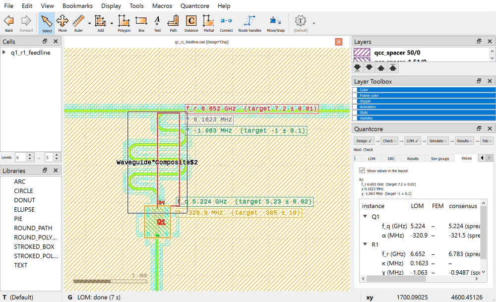
Values on the layout for a Q1 + R1 chip after Run LOM (the targets were chosen to show all three colours).
9. Simulate, export only
Press Simulate in the Flow strip. You do not need to select anything: with nothing selected, the dialog offers the first qubit with its readout. Press Export the job only. This writes the job folder, with the geometry and the AEDT scripts, and does not solve it.
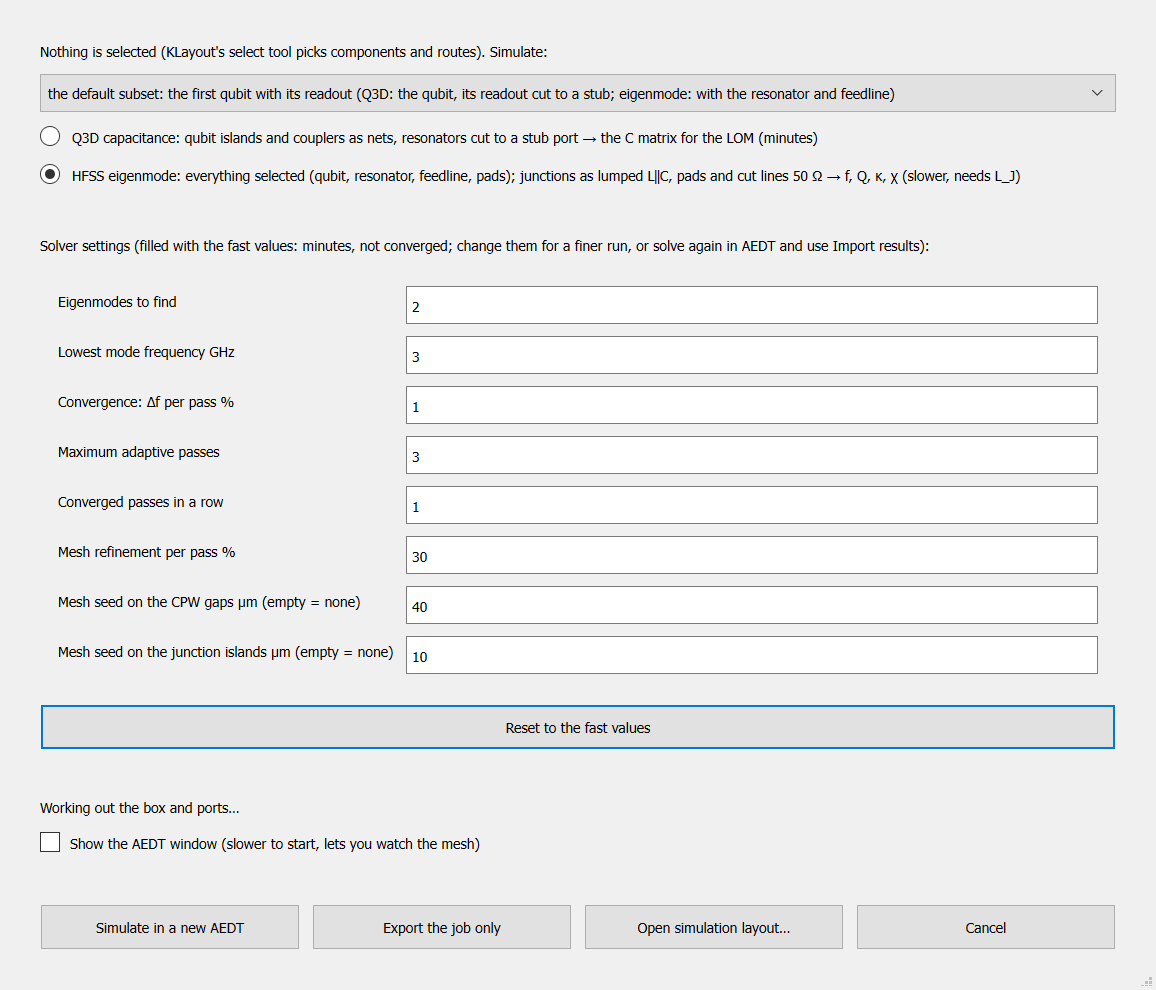
The Simulate dialog. Export the job only writes the job folder without a solve.
10. Export for fab
Click Fab > Export for fab (mask, netlist, design.py, PNG)… and choose a folder. The export warns first if Check
found errors, and it refuses while a route has failed. It writes <name>_fab.oas, circuit.json, design.py and a PNG.
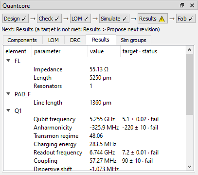
The panel after Export for fab: the Fab step is done.
Where next
Q1 + R1 tutorial: every step with all values and the reasons for them.
Place and route: placing, snapping, routes, hangers and sim groups.
The Flow strip: Check, LOM, Simulate, Results and Fab from the panel.
Tutorials: the Python tutorials.