IBM 5-qubit bowtie
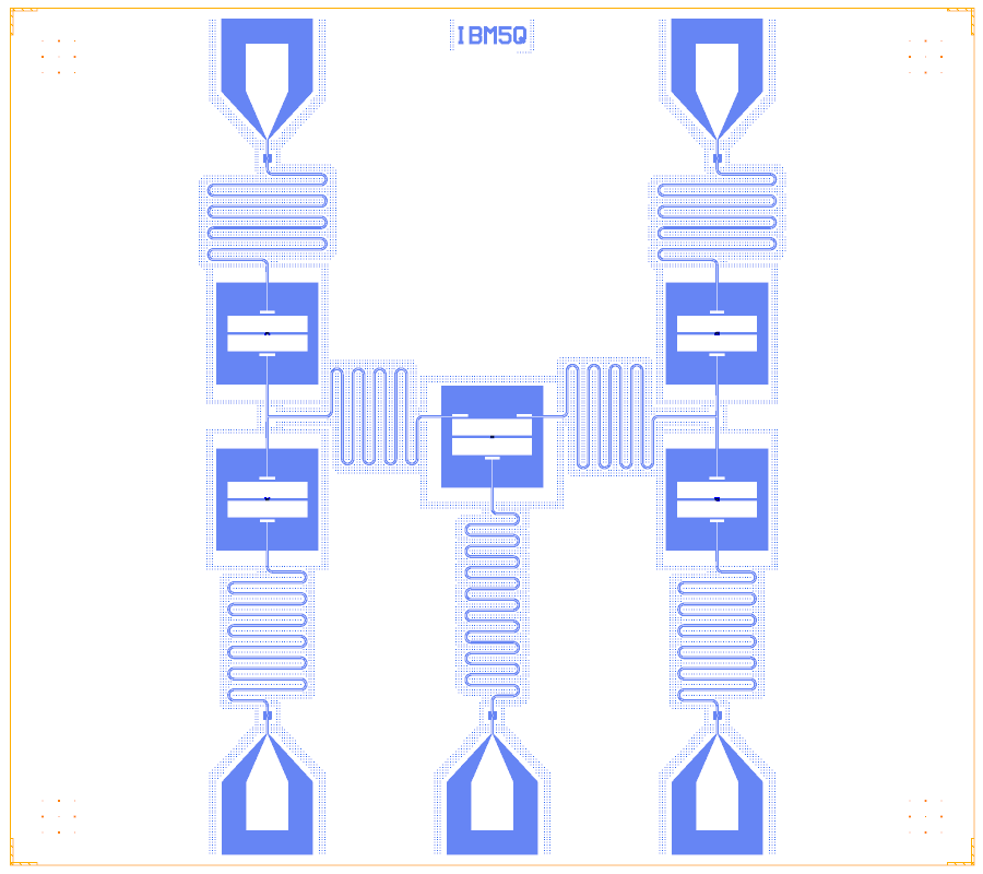
IBM’s first cloud processor (ibmqx2 Yorktown, ibmqx4 Tenerife): five fixed-frequency transmons and two bus resonators, each bus coupling three qubits, so the coupling graph is two triangles sharing Q2. Each qubit has its own readout resonator and line. No layout is public; IBM’s device data give the topology and targets, and the layout is ours.
This notebook shows the multi-qubit bus (a λ/2 line from Q2 to a tee whose two short stubs reach the other two qubits) and junctions sized qubit by qubit with the LOM.
At a glance
Notebook |
|
Source |
IBM published device data (coupling map, frequencies); no public layout |
Chip |
9 × 8 mm Quantcore die, sapphire 650 µm (εr 10.25) |
On the chip |
5 pocket transmons · 5 λ/2 readouts · 2 tees and 2 three-qubit buses · 5 finger capacitors · 5 bond pads |
Builds today |
yes (layout built on 2026-11-19 in 10 s) |
How the notebook builds it
Each Design segment is one cell with a picture of the chip so far (see the notebook template).
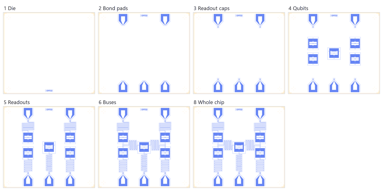
Die. A 9 × 8 mm die with the QCT frame and the device ID
IBM5Q.Bond pads. One readout pad per qubit, on the top and bottom edges.
Readout caps. The five series finger capacitors and their short 50 Ω lines.
Qubits. Five
TransmonPocket6pockets with Quantcore trilayer junctions.Readouts. Five λ/2 meanders from the qubits to the capacitors.
Coupling. Two tees and the two three-qubit λ/2 buses.
Control lines. None: each qubit is driven through its own readout line.
Whole chip. The centring check, targets, sim groups and the save.
LOM estimates
Numbers are from a run of this notebook on 2026-11-19 (Setup, Design, Check and the LOM cells, 239 s): QuCat normal modes with QuTiP dressed values.
group |
qubit |
f_q (GHz) |
α (MHz) |
resonator |
f_r (GHz) |
κ (MHz) |
χ (MHz) |
|---|---|---|---|---|---|---|---|
Q0+R |
Q0 |
5.268 |
-145 |
R_Q0 |
6.429 |
0.908 |
-0.888 |
Q1+R |
Q1 |
5.224 |
-146 |
R_Q1 |
6.381 |
0.888 |
-0.878 |
Q2+R |
Q2 |
5.028 |
-143 |
R_Q2 |
6.337 |
0.871 |
-0.737 |
Q3+R |
Q3 |
5.269 |
-145 |
R_Q3 |
6.476 |
0.929 |
-0.841 |
Q4+R |
Q4 |
5.089 |
-147 |
R_Q4 |
6.428 |
0.909 |
-0.687 |
pair |
f_a (GHz) |
f_b (GHz) |
J (MHz) |
target J (MHz) |
ZZ (kHz) |
|---|---|---|---|---|---|
Q0-Q1 |
5.268 |
5.224 |
1.8 |
1.91 |
76 |
Q0-Q2 |
5.268 |
5.032 |
1.61 |
1.82 |
-30 |
Q1-Q2 |
5.223 |
5.032 |
1.55 |
1.24 |
-63.1 |
Q2-Q3 |
5.031 |
5.267 |
1.56 |
1.82 |
-45.9 |
Q2-Q4 |
5.031 |
5.088 |
1.57 |
1.81 |
69.6 |
Q3-Q4 |
5.268 |
5.088 |
3.78 |
2.01 |
-173 |
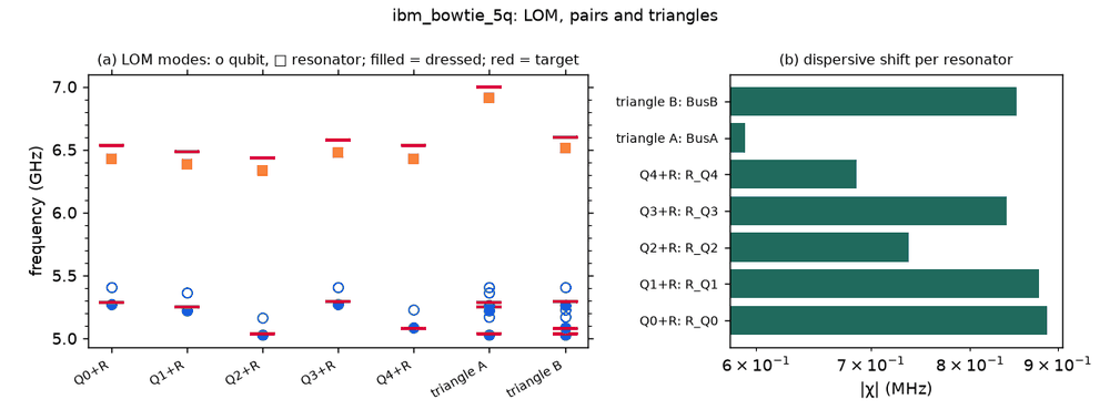
These are lumped-model estimates (component formulas and calibration), not FEM results. The LOM page says how far to trust them.
Build spec
The rest of this page is the detailed spec the notebook was built from, with every component, port, route and length.
Sources.
Device data (primary): Qiskit
FakeYorktownbackend filesconf_yorktown.json/props_yorktown.jsonfromqiskit-ibm-runtime(qiskit_ibm_runtime/fake_provider/backends/yorktown/, Apache-2.0; snapshot of ibmqx2, 2021-03-15; local copybuild/external/qiskit_fake_backends/). Hamiltonian (Duffing model, vars in rad/ns ÷ 2π): f_q = 5.2823 / 5.2475 / 5.0334 / 5.2920 / 5.0785 GHz, α = −330.8 / −330.4 / −376.1 / −329.7 / −333.1 MHz, J (MHz): 0-1 1.905, 0-2 1.820, 1-2 1.236, 2-3 1.820, 2-4 1.812, 3-4 2.009; coupling map 0-1, 0-2, 1-2, 2-3, 2-4, 3-4; measurement LO ranges centred at 6.5304 / 6.4817 / 6.4365 / 6.5789 / 6.5301 GHz.Buses: “two superconducting CPWs, one coupling Q2, Q3 and Q4 and another one coupling Q0, Q1, Q2 with resonator frequencies 6.6 GHz and 7.0 GHz” and the ibmqx4 table (readout 6.439–6.580 GHz, χ 408–512 kHz): Dash et al., arXiv:1805.10478 (2018), citing IBM’s (now removed)
ibmqx-backend-informationREADME for ibmqx4.Architecture: each qubit with its own CPW readout resonator, qubits coupled through bus resonators: Córcoles et al., Nat. Commun. 6, 6979 (2015) (arXiv:1410.6419; local copy
build/external/corcoles2015/).
Licence. Apache-2.0 data (compatible with the repository’s GPL); papers cited. No layout of the chip is public (searched GitHub, IBM/Qiskit repositories, Qiskit Metal, SQuADDS); the layout and code are ours.
What it is. Five fixed-frequency floating transmons; bus A (λ/2) from Q2 to a tee whose two 150 µm stubs reach Q0 and Q1, bus B from Q2 to a tee reaching Q3 and Q4; a λ/2 readout per qubit to a series finger capacitor and its own 50 Ω pad (IBM drove and read each qubit through its readout line).
Chip. 9 × 8 mm, Quantcore die frame (QCT), device ID IBM5Q; sapphire 650 µm, εr 10.25; 10/6 µm CPW.
Junctions: Quantcore trilayer (junction_type="Quantcore Junction"), L_J 6.07–6.63 nH (R_n 40.6–44.3 kΩ).
Notebook. examples/designs/ibm/ibm_bowtie_5q.ipynb.
Components
instance |
catalog ref |
key params (µm) |
at (x, y) |
notes |
|---|---|---|---|---|
Q0 … Q4 |
metal:TransmonPocket6 |
pads 750 × 160, gap 20, pocket 950; bus pads 150 wide, readout pads 140 |
Q2 (4500, 4000); Q0/Q1 (2400, 4965 / 3415); Q3/Q4 (6600, 4965 / 3415) |
Quantcore Junction, L_J per qubit |
TA, TB |
metal:LineTee |
(2400, 4190), (6600, 4190) |
the bus forks |
|
C_Q0 … C_Q4 |
FingerCapacitorSquare (KQC) |
defaults |
250 µm before each pad |
readout coupling |
P_Q0 … P_Q4 |
BondPad |
top (Q0, Q3), bottom (Q1, Q2, Q4) |
50 Ω |
Routes
route |
from → to |
type, length (µm) |
notes |
|---|---|---|---|
BusA, BusB |
Q2.bw / Q2.be → TA / TB |
meander 8190 / 8750 |
λ/2, 7.0 / 6.6 GHz targets |
BusA_Q0, BusA_Q1, BusB_Q3, BusB_Q4 |
tee → outer qubit bus pad |
cpw 150 |
stubs (wires in the LOM) |
R_Q0 … R_Q4 |
readout pad → finger cap |
meander 9348–9562 |
λ/2 readouts |
L_Q* |
finger cap → pad |
cpw 213.5 |
LOM node structure
Floating pockets: Qn.island1/2 + trilayer JJ; bus pads → one node per bus (Q2’s pad, the tee and both outer pads
joined; λ/2 TLres); readout pad → λ/2 TLres → finger-cap π network → 50 Ω pad.
Targets and LOM values
quantity |
IBM |
rebuild (LOM) |
|---|---|---|
f_q |
5.033–5.292 GHz |
5.028–5.269 GHz (within 5–23 MHz per qubit; L_J solved) |
α |
−330 … −376 MHz |
≈ −145 MHz (PDK: R_n ≤ 50 kΩ → L_J ≤ 7.5 nH, so C_Σ ≈ 130 fF) |
buses |
7.0 / 6.6 GHz |
7.020 / 6.613 GHz (triangle groups) |
readout |
6.437–6.579 GHz |
within 1 MHz, κ 0.90–0.96 MHz, χ −0.62 … −0.78 MHz |
J |
1.24–2.01 MHz |
1.45–1.51 MHz on the four Q2 pairs, 2.39 / 2.72 MHz on Q0–Q1 / Q3–Q4; ZZ −26 … −151 kHz |
Simplifications / adaptations
The three-qubit bus is a λ/2 with a forked end (the true IBM geometry is not public); in the LOM the bus is one node, the fork stubs (2 × 150 µm) are not in its length (the eigenmode job holds them).
α about half of IBM’s (PDK junction window); the CR-gate collision windows scale with α.
One readout line per qubit (IBM QX style), no Purcell filter, no flux lines (fixed-frequency qubits).