DaisyWoven bump test
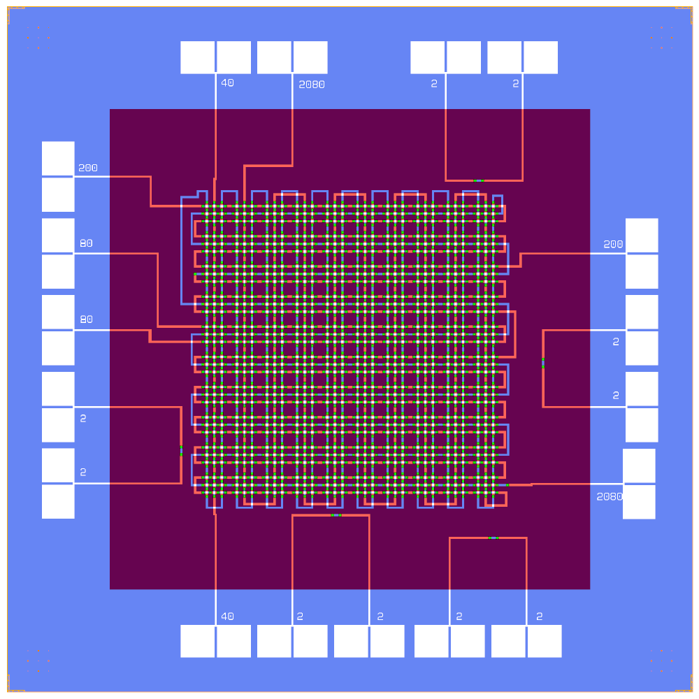
A flip-chip test chip from KQCircuits. The same daisy-chain pattern is drawn on both faces (metal, under-bump metallization (UBM) and indium bumps), with probe pads around the edge. After bonding you measure the DC resistance of each chain. There are no qubits, resonators or RF lines.
The layout is one KQC cell, rebuilt on the Quantcore PDK (sapphire, Quantcore die frame). Build it to see how a whole static KQC chip cell is placed in a Designer and how the bottom and top faces of a flip chip are drawn.
At a glance
Notebook |
|
Source |
KQCircuits |
Chip |
10 × 10 mm, two faces ( |
On the chip |
one static pattern: daisy chains with 2, 40, 80, 200 and 2080 bumps, probe pads, UBM and indium bumps on both faces |
Builds today |
yes (layout built on 2026-11-19 in 5 s) |
How the notebook builds it
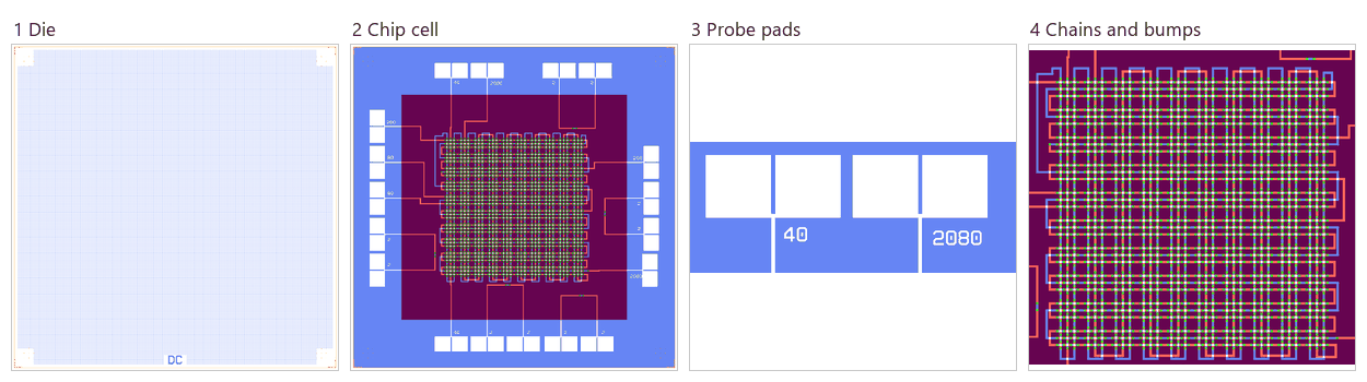
Die. The empty 10 × 10 mm chip with the Quantcore frame (dicing marks, alignment grids, chip boundary, device ID) and the device ID “DC”.
Chip cell. One instance: KQC’s
DaisyWovenat the chip origin, with KQC’s own frame turned off.Probe pads. A view of the pads, which are part of the static pattern, with the pad rule.
Chains and bumps. A view of the daisy chains and the bump counts per face.
LOM estimates
This chip has no lumped-model estimate. The daisy chains are DC test structures with no LOM model, so the netlist is ground only and has no modes. The chip’s numbers are the bump counts of Design 4.
Build spec
The rest of this page is the detailed spec the notebook was built from: every component, port, route and length.
Source other-libs/KQCircuits-main/KQCircuits-main/klayout_package/python/kqcircuits/chips/daisy_woven.py
(DaisyWoven, chip name “DC”), GPL-3.0 (IQM Finland). The pattern is the static KQC cell
kqcircuits/elements/daisy_woven.oas. What it is: a process test for flip-chip indium bumps. The same
hand-drawn daisy-chain pattern goes on both faces: metal, underbump metallization (UBM) and indium bumps, plus pixel
corner texts, dicing edge and launcher-like pads drawn in the static file. No qubits, no resonators. 10 × 10 mm,
frames_enabled=[0,1], KQC frame = Designer frame. The static-cell import with layer remap and polarity inversion is
handled by the KQC chip PCell (see the rebuild below).
Components
instance |
catalog ref |
key params (units) |
at (x, y) |
rot |
notes |
|---|---|---|---|---|---|
daisy (face 0 and face 1) |
|
static layers 11/1 (+30 per face), 32/4 (+30), 33/4 (+30) |
moved by (W/2, H/2) × 1e3 dbu = chip centre |
0 |
KQC copies them to |
Routes
None. The scratch KQC build has no element instances, only the chip frames and static shapes.
Launchers, pads, test structures, markers, labels
All of these are in the static pattern. Chip frames on both faces come from the KQC Chip base
(produce_structures).
LOM node structure (qubit ↔ resonator ↔ feedline ↔ bus ↔ control lines)
None (DC resistance test).
Targets (if stated)
None.
Simplifications for a first rebuild
Not needed for the circuit flow. If wanted, export the KQC-built DaisyWoven cell to OAS and place it as static:<path>.
That needs a dummy port, because static: cells require at least one, or a schema change allowing port-less static
cells. Keep the KQC layer mapping (1t1/2b1 metal, UBM, indium).
Quantcore PDK rebuild
The notebook is a Quantcore-PDK rebuild of the source chip. The netlist, LOM and imported components are kept, and the process is Quantcore’s.
Notebook: examples/designs/kqc/daisy_woven.ipynb.
Chip: the Quantcore die frame (L dicing markers 1000/0, 3 × 3 alignment grids 1001/0, chip boundary 100/0, device ID where an edge is free; any brand text is QCT), drawn on the source’s 10 × 10 mm chip. The KQC chip PCell is placed with
frames_enabled=[], so its own ChipFrame (dicing edge, markers, labels) is not drawn. The chip parameter ischeese: "chip"(the PDK squares over the whole die), but this chip has no ground plane: theDaisyWovencell etches the whole chip box except its pattern, and its probe pads are isolated metal, so they stay solid and no hole is drawn. The top chip (face 2b1) gets no frame, because PDK v3 defines none for the flip-chip top chip (its layers export to 800–804/0).Stack: sapphire 650 µm, εr 10.25 (the PDK default stack, used by the LOM estimates and every FEM export); KQC’s own simulation default is silicon (εr 11.45), so LOM capacitances and resonator frequencies here are for sapphire.
Junctions: none on this chip (indium bumps and UBM only).
Kept: the whole KQC chip PCell with the source’s parameters (KQC’s own
build()) (the static daisy pattern, its polarity inversion, the UBM and indium layers: 802/0, 801/0).