Resonator test chip (QPDK)
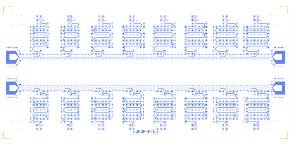
Sixteen shorted λ/4 resonators on two straight probelines, eight per line, for measuring losses. The layout comes from QPDK’s resonator_test_chip.py (MIT) and is rebuilt on the Quantcore PDK; the rebuild is GPL-3.0. The chip has no qubits.
This notebook is an example of many hanger resonators on a line, resonators without a qubit (open ends instead), and a chip wider than the standard die.
At a glance
Notebook |
|
Source |
gdsfactory |
Chip |
9.2 × 4.3 mm (the source’s size, not the 7.5 mm die), CPW 10 / 6 µm |
On the chip |
4 launchers · 2 probelines · 16 open ends · 16 λ/4 resonators (200 µm coupled section each) |
Builds today |
yes (layout built on 2026-11-19 in 6 s) |
How the notebook builds it
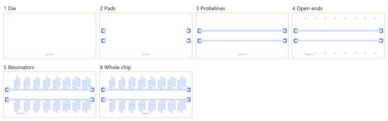
Die. The 9.2 × 4.3 mm chip with the frame and the device ID.
Bond pads. Four launchers on the 100 µm pad rule.
Probelines. Two straight lines from launcher to launcher.
Open ends. Sixteen 6 µm open ends, where the resonators start (the chip has no qubits).
Resonators. Sixteen meandered λ/4 resonators, each ending in a shorted coupled section on its probeline.
Coupling. Only the hanger sections; nothing else couples them.
Control lines. None.
Whole chip. One sim group per probeline, centring, save.
LOM estimates
Numbers are from a run of this notebook on 2026-11-19 (Setup, Design, Check and the LOM cells, 74 s): QuCat normal modes with QuTiP dressed values.
mode |
kind |
f (GHz) |
κ (MHz) |
A (MHz) |
participation |
|---|---|---|---|---|---|
RB8 |
resonator |
6.28 |
0.102 |
0 |
RB8 1.00 |
RB7 |
resonator |
6.541 |
0.116 |
0 |
RB7 1.00 |
RB6 |
resonator |
6.824 |
0.131 |
0 |
RB6 1.00 |
RB5 |
resonator |
7.133 |
0.15 |
0 |
RB5 1.00 |
RB4 |
resonator |
7.472 |
0.172 |
0 |
RB4 1.00 |
RB3 |
resonator |
7.844 |
0.199 |
0 |
RB3 1.00 |
RB2 |
resonator |
8.255 |
0.232 |
0 |
RB2 1.00 |
RB1 |
resonator |
8.711 |
0.272 |
0 |
RB1 1.00 |
mode |
kind |
f (GHz) |
κ (MHz) |
A (MHz) |
participation |
|---|---|---|---|---|---|
RT8 |
resonator |
6.158 |
0.0964 |
0 |
RT8 1.00 |
RT7 |
resonator |
6.408 |
0.109 |
0 |
RT7 1.00 |
RT6 |
resonator |
6.68 |
0.123 |
0 |
RT6 1.00 |
RT5 |
resonator |
6.976 |
0.14 |
0 |
RT5 1.00 |
RT4 |
resonator |
7.299 |
0.16 |
0 |
RT4 1.00 |
RT3 |
resonator |
7.653 |
0.185 |
0 |
RT3 1.00 |
RT2 |
resonator |
8.044 |
0.215 |
0 |
RT2 1.00 |
RT1 |
resonator |
8.477 |
0.251 |
0 |
RT1 1.00 |
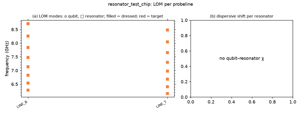
These are lumped-model estimates (component formulas and calibration), not FEM results. The LOM page says how far to trust them.
Build spec
The rest of this page is the detailed spec the notebook was built from, with every component, port, route and length.
Source: qpdk/samples/resonator_test_chip.py
(resonator_test_chip_python, filled_resonator_test_chip) and its frozen netlist
resonator_test_chip_yaml.pic.yml · licence MIT (verified) · Read on 2026-11-02. Image docs/_static/images/resonator_test_chip.png.
What it is: two straight west→east probelines, 1000 µm apart, each with two launchers. Each carries 8 shorted λ/4
CPW resonators (quarter_wave_resonator_coupled, 6 meanders, 200 µm coupled section). The bottom-line resonators hang
below the line and the top-line ones (mirrored) sit above it. The README says “systematically varied CPW widths and gaps”,
but both the code and the YAML use one cross-section (10/6 µm) and vary only length. It serves as a loss and kinetic-inductance chip.
Frame: source x 0…9000, y about −1250…+2250 (meander height ≈ 1250 µm, read from the image). The filled version’s
chip edge is (xsize + 200, ysize + 800) at (xmin − 100, ymin − 400), so box (0, 0, 9200, 4300) and
Designer = source + (100, 1650). Si, M1 negative.
The chip needs only BondPad and routes: the resonators are plain λ/4 hangers, which the route model covers directly.
Components
instance |
catalog ref |
key params |
at (x, y) Designer |
rot |
notes |
|---|---|---|---|---|---|
PW_B |
|
default |
(100, 1650) |
270 (faces east) |
source probe_west_bot (0, 0) |
PE_B |
|
default |
(9100, 1650) |
90 (faces west) |
probe_east_bot (9000, 0), mirrored |
PW_T |
|
default |
(100, 2650) |
270 |
probe_west_top (0, 1000) |
PE_T |
|
default |
(9100, 2650) |
90 |
probe_east_top (9000, 1000) |
No qubits. The chip is resonators only. |
Routes
Probelines are straight. QPDK adds a small S-bend at each launcher because the probeline sits 26 µm off the launcher axis; we skip it. Coupled section in the YAML: coupling_gap 16 µm edge-to-edge (centre spacing 26 µm), so ground_gap = 4 µm. The Python default is coupling_gap 4 µm, which merges both CPW gaps (no ground strip). Use the YAML value. Resonator k (k = 1…8) has its 200 µm coupled section at source x 1000k…1000k + 200, so the Designer centre is x = 1000k + 200 and s_k = 1000k − 200 from the pad port (≈ x 400). The shorted end is the west end of the coupled section, then the line meanders away. Use direction backward (the route arrives from the east end and the short lands at the west end).
route |
from → to |
type, length |
hanger (s, length, side, ground_gap, direction) |
notes |
|---|---|---|---|---|
FL_B |
PW_B.a → PE_B.a |
cpw |
straight y 1650 |
|
FL_T |
PW_T.a → PE_T.a |
cpw |
straight y 2650 |
|
RB1…RB8 |
free_end (meander start) → FL_B.hanger |
meander 3600, 3800, 4000, 4200, 4400, 4600, 4800, 5000 |
s 800, 1800, …, 7800; 200; right; 4; backward |
resonators below FL_B |
RT1…RT8 |
free_end → FL_T.hanger |
meander 3700, 3900, 4100, 4300, 4500, 4700, 4900, 5100 |
s 800, 1800, …, 7800; 200; left; 4; backward |
resonators above FL_T |
Lengths come from np.linspace(0.9·4000, 1.275·4000, 16) (100 µm steps), interleaved: even indices on the bottom,
odd on the top. The open end is a free end: start each resonator route at Designer.free_end(at, dir, term=6),
≈1250 µm from the line on its side, at x ≈ 1000k + 100. Let the meander fill the 1250 × ~600 µm cell.
Launchers, pads, test structures, markers, labels
4 launchers. The filled version adds a 100 µm chip edge and 15 µm vortex squares (70 µm gap, stagger 2), which maps
to chip={"with_grid": True}.
LOM node structure
FL_B and FL_T: one conductor each, two 50 Ω ports. Each RBk/RTk is an independent λ/4 resonator with coupled-line κ to its probeline. No qubits, buses or control lines.
Targets
None stated in the code. λ/4 on Si (ε_eff ≈ 6.2): f ≈ 3.0 GHz·mm / L, so 8.3 GHz (3600) down to 5.9 GHz (5100), about 0.1–0.2 GHz apart. The README shows a SAX sweep from 4 to 10 GHz resolving all eight notches per line.
Simplifications for a first rebuild
No S-bends, no fill. Each resonator is
d.route(name, Designer.free_end(at, dir, term=6), FL.hanger(...), meander=L). The schema allows a free end asfromand a hanger only asto.A CPW width/gap sweep (as the README describes) can be added later by giving each resonator route its own
a/b.
Build
The notebook is examples/designs/qpdk/resonator_test_chip.ipynb. Each resonator starts at a 6 µm CpweOpenEnd (a route from a free end to a hanger has no LOM start node). Resonator routes use r = 75 µm so 6 meanders fit in 1250 µm.
Quantcore PDK rebuild
The notebook is a Quantcore PDK rebuild, not a replica: the netlist, LOM and imported components are kept, the process is Quantcore’s.
Notebook: examples/designs/qpdk/resonator_test_chip.ipynb.
Chip: the Quantcore die frame (L dicing markers 1000/0, 3 × 3 alignment grids 1001/0, chip boundary 100/0, device ID where an edge is free; any brand text is QCT), drawn on the source’s 9.2 × 4.3 mm chip (the design does not fit the 7.5 mm die); no KQC chip frame.
Stack: sapphire 650 µm, εr 10.25 (the PDK default stack, used by the LOM estimates and every FEM export); QPDK’s process is Al on Si (εr 11.45), so frequencies are not the QPDK ones.
Junctions: none on this chip (resonators only).
Kept: the topology and every component with the source’s parameters and positions, the readout / resonator lengths and coupled sections, the sim groups (the 16 lengths 3600–5100 µm, the 1000 µm pitch, 6 meanders).