Five-Xmon chip (chip_01)
Three Quantcore chips share this page: a 7.5 mm die with five Xmon qubits, each read out by its own quarter-wave
resonator hanging off one feedline. chip_01 is the first version (SQUID qubits), chip_01_creator the later one
with single trilayer junctions that was swept over 16 junction sizes on a wafer, and chip_01_4x4 tiles sixteen
copies of the die for a wafer. They are Quantcore’s own earlier chips, from the QWri legacy scripts chip_01.py,
chip_01_creator.py and chip_01_4x4.py, made to find which junction size puts the qubits in the 4 to 8 GHz band.
The rebuild draws the same chip from Quantcore PDK parts: the resonator tails now run into the qubit claws, the bond pads sit 100 µm from the die edge, and the PDK adds its frame and cheese band. Build this one to see how a feedline chip with several qubits is laid out and how a legacy script maps to a Designer JSON.
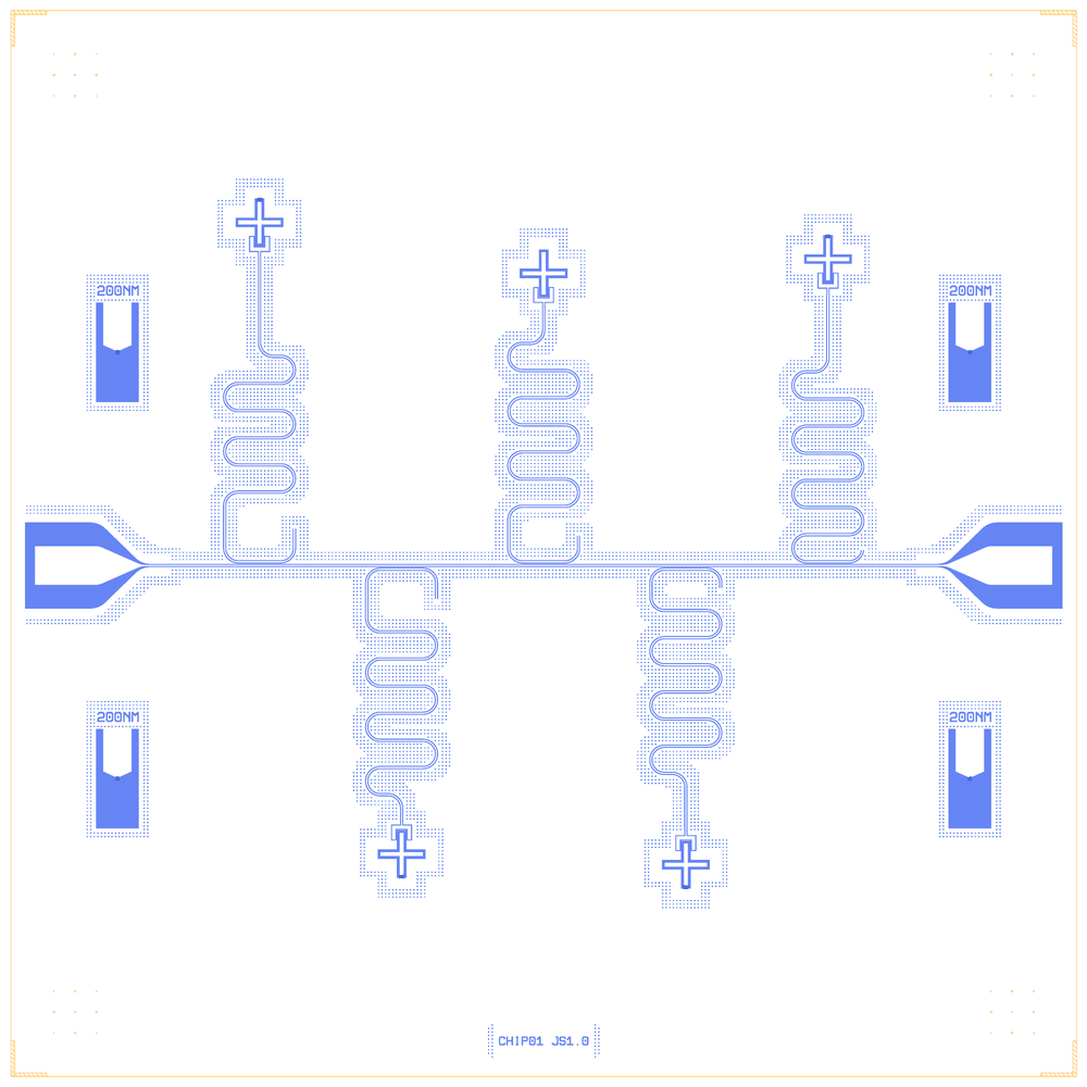
chip_01_creator as rebuilt on the Quantcore PDK: feedline in the middle, resonators above and below, an Xmon at each resonator end
At a glance
chip_01 |
chip_01_creator |
chip_01_4x4 |
|
|---|---|---|---|
Notebook |
|
|
|
Source script |
|
|
|
Chip |
7.5 × 7.5 mm die, 10/6 µm CPW |
same |
30 × 30 mm, sixteen 7.5 mm dies |
On the chip |
5 Xmons (4 SQUIDs) · 5 λ/4 resonators · 8 junction test pads |
5 Xmons (4 single junctions) · 5 λ/4 resonators · 4 junction test pads |
16 copies of the |
Builds today |
yes, rebuilt from its JSON on 2026-11-19 in 2.8 s (the notebook itself was not re-run) |
yes, rebuilt from its JSON on 2026-11-19 in 4.0 s (the notebook itself was not re-run) |
yes, the die: rebuilt from its JSON on 2026-11-19 in 3.2 s (the notebook itself was not re-run) |
Pictures
chip_01 (SQUIDs)
The first version: every Xmon at y = ±2250 µm with a SQUID, eight test pads along the edges. Left, the original legacy layout; right, the Quantcore rebuild.
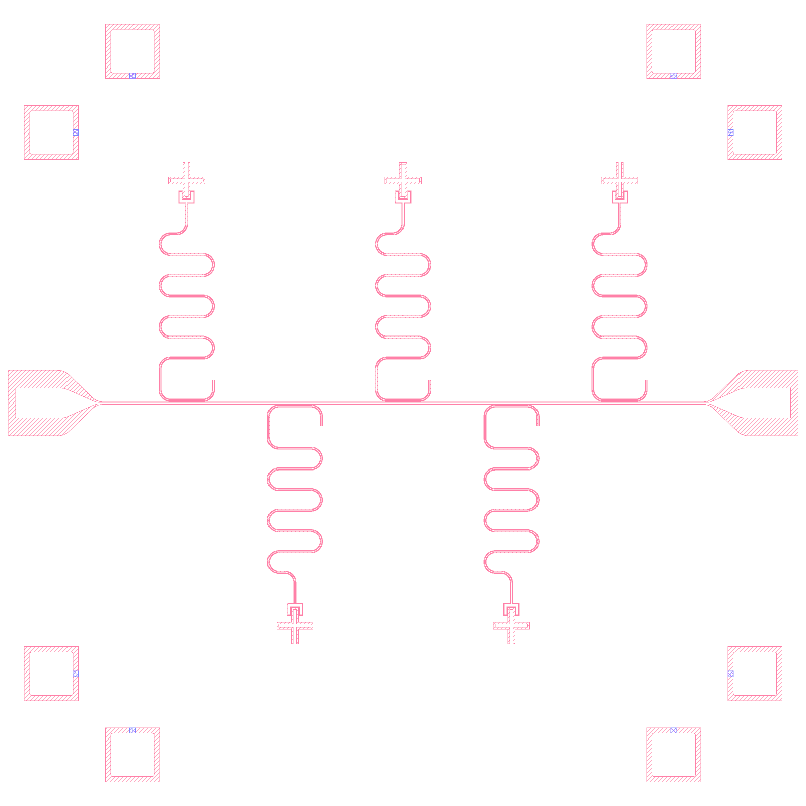
chip_01: the original legacy layout (render of the legacy GDS)
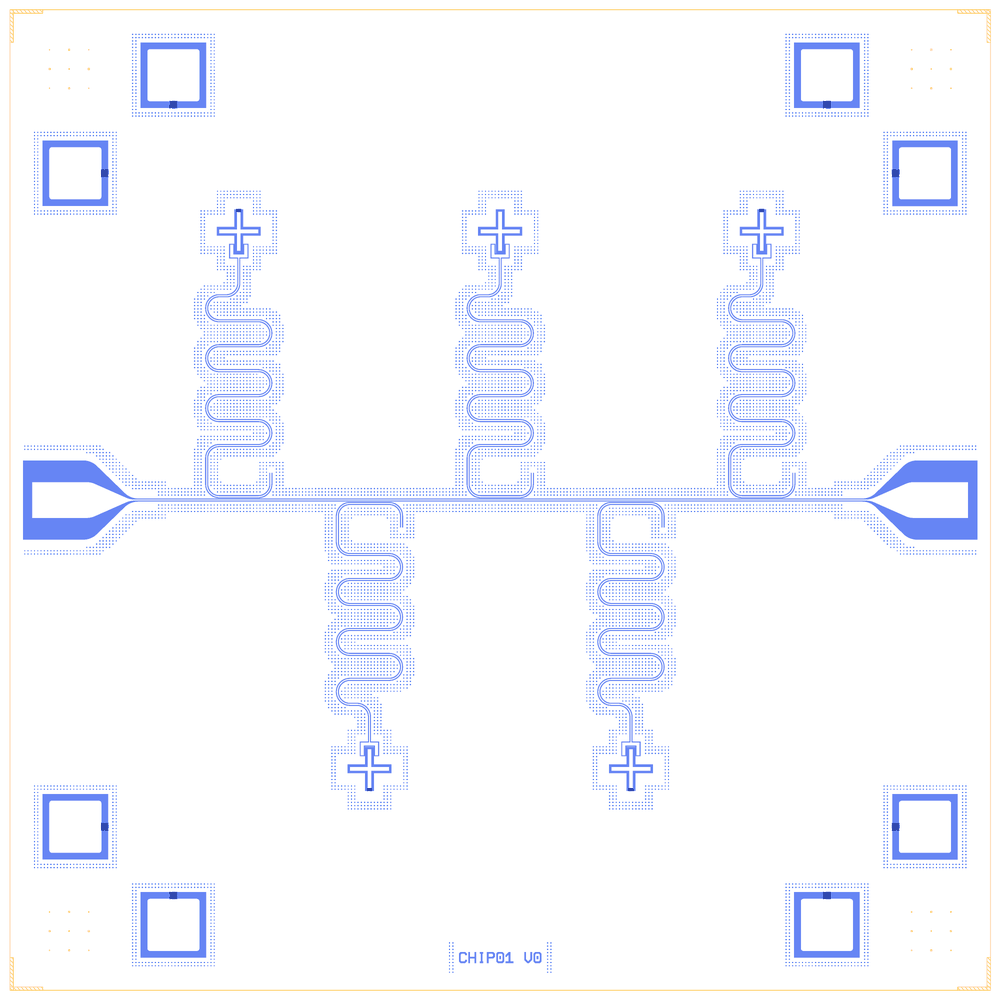
chip_01: the Quantcore rebuild
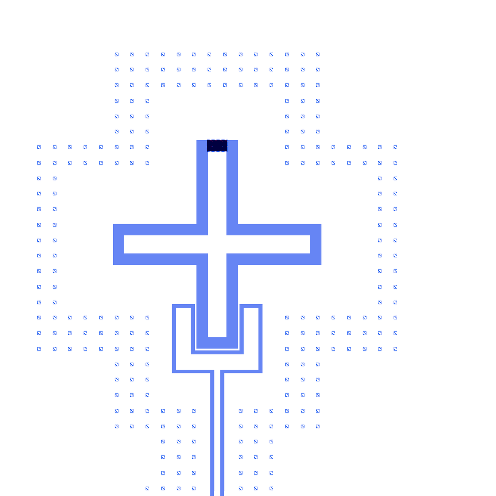
One Xmon: the cross, its claw at the bottom taking the resonator tail, and the junction at the tip of the north arm
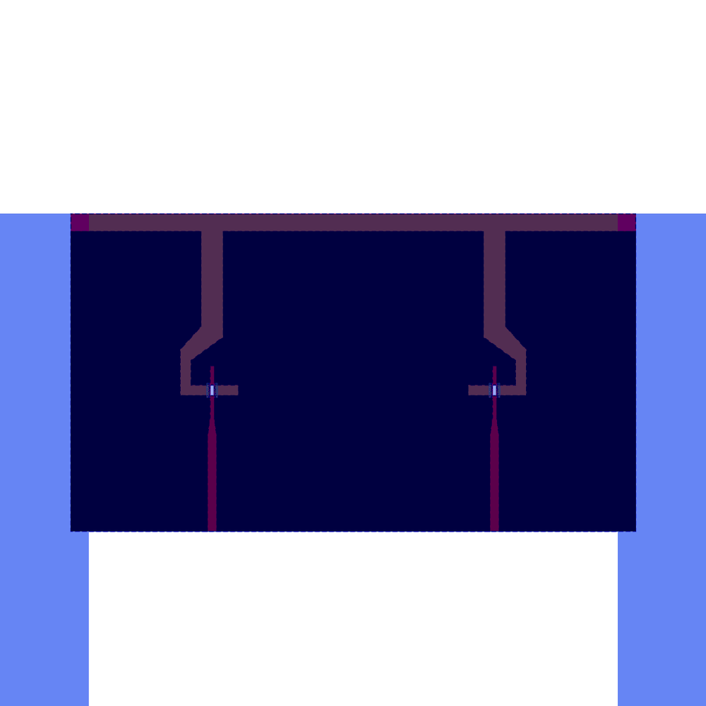
Close-up (40 µm box) of the junction layers at the tip of the north arm
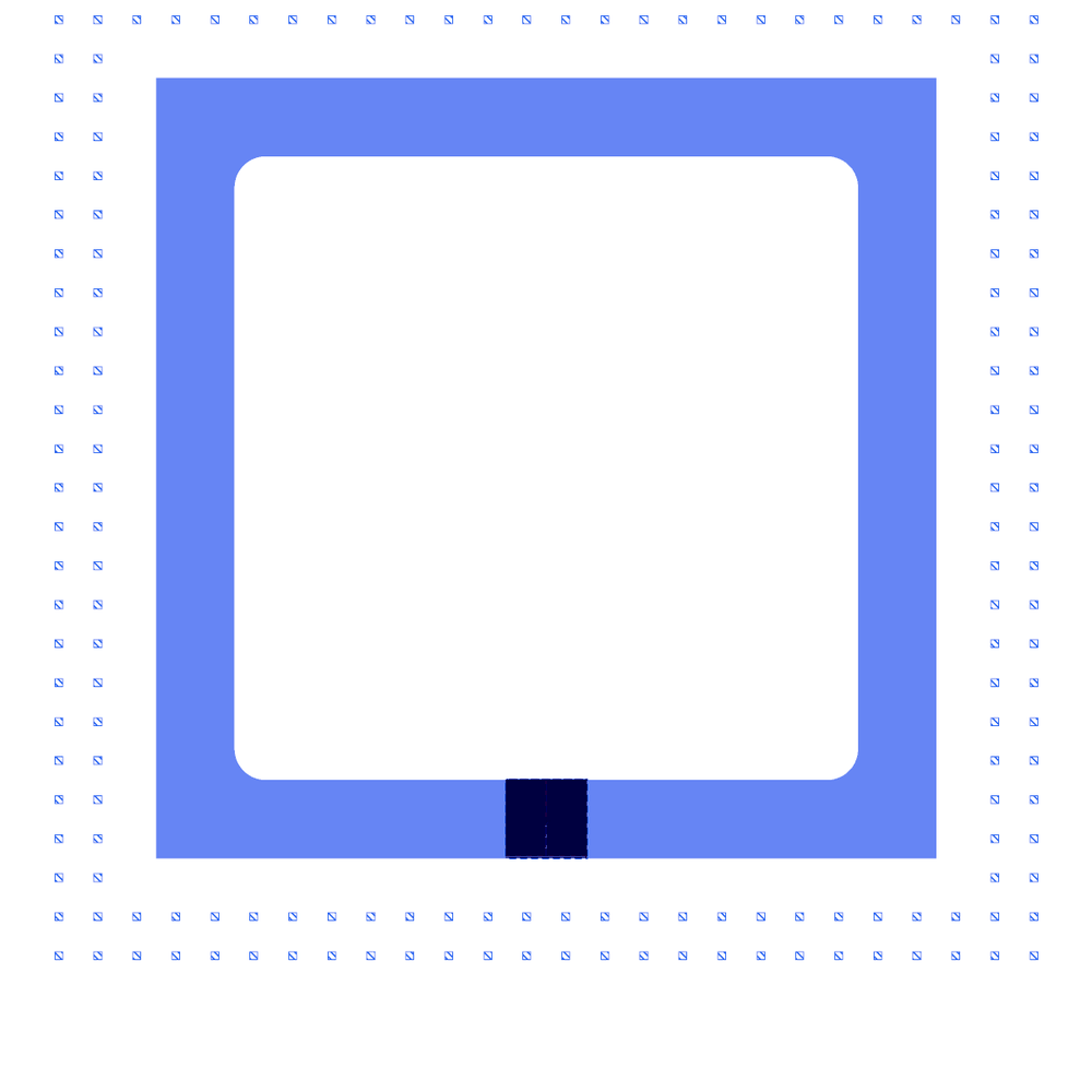
A junction test pad: a pad in a ground ring with a junction at its foot
chip_01_creator (single junctions)
The JS-sweep chip: the same layout with different resonator necks and Xmon heights, a single trilayer junction per
qubit and four testPad_AVAQUS test pads whose label carries the junction scale (JS).
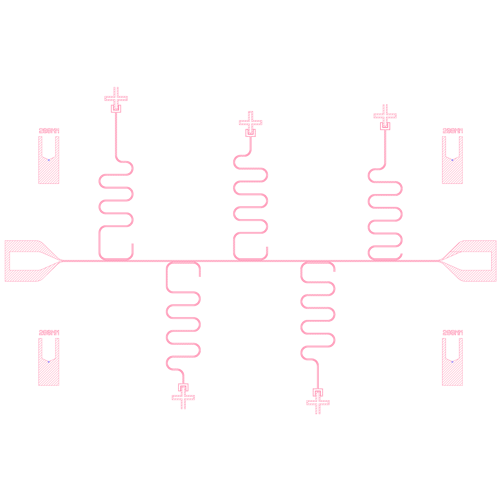
chip_01_creator: the original legacy layout (render of the legacy GDS)
chip_01_creator: the Quantcore rebuild
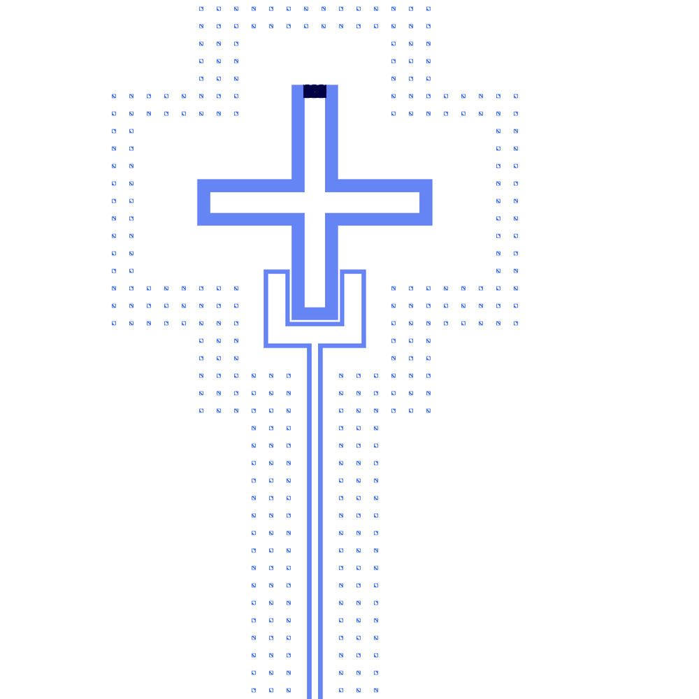
One Xmon with its claw and resonator tail: the tail is the open end of the quarter-wave resonator
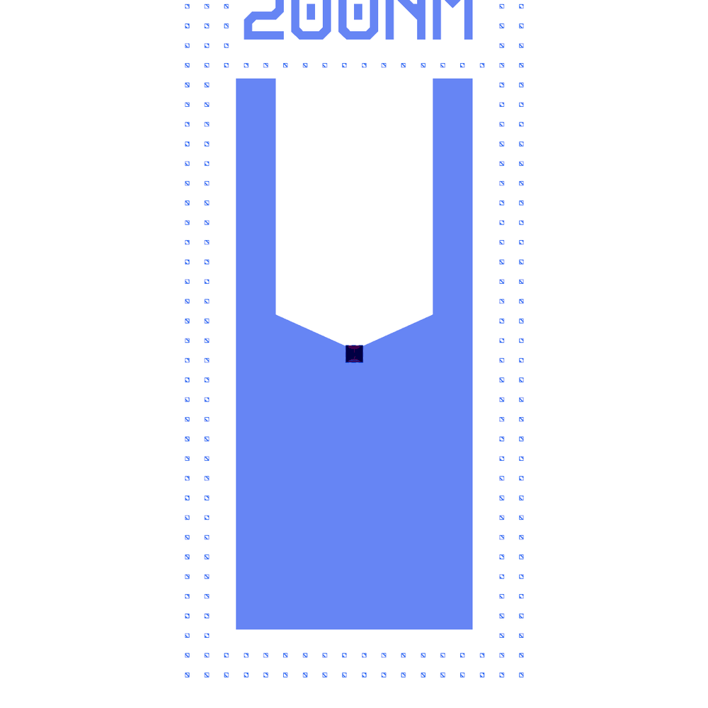
A test pad with its label (200 nm finger width at JS = 1.0)
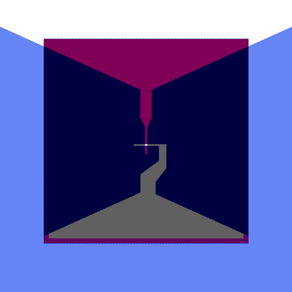
The test-pad junction (30 µm box): bottom finger, top finger and their overlap in white
chip_01_4x4 (wafer tiling)
Not a new chip: the chip_01 die repeated 4 × 4 at a 7.5 mm pitch (30 × 30 mm). The legacy script placed the copies
at only four positions; the rebuild uses the sixteen intended ones. The first picture is a montage of the rebuilt die.
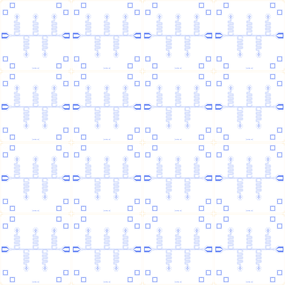
chip_01_4x4: the rebuilt die tiled 4 × 4 (montage of the die render)
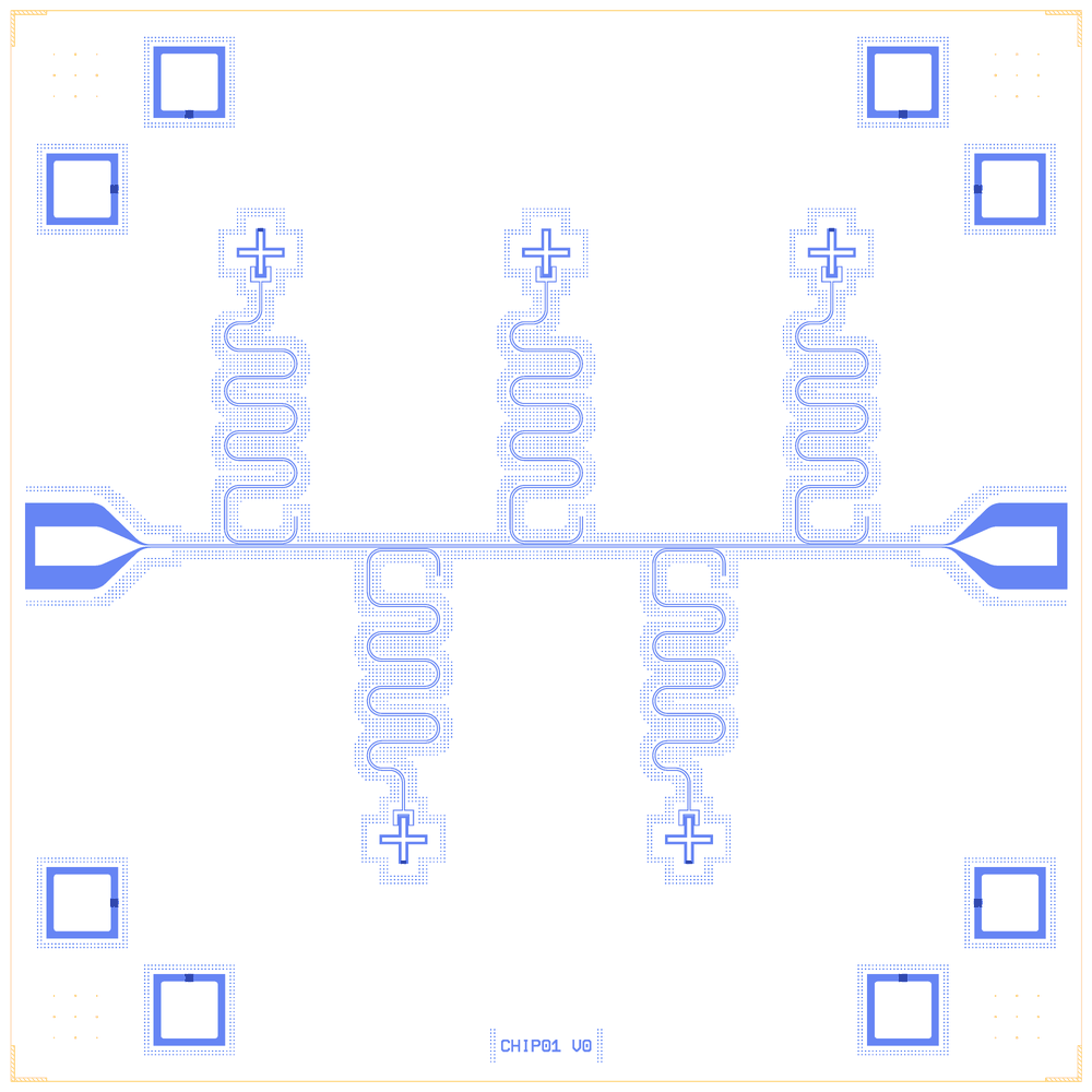
The die that is tiled: chip_01 as saved in chip_01_4x4/die.json
LOM estimates
The notebook’s saved outputs hold no LOM run (its LOM cells were not executed), so there are no estimates to show here and none were computed for this page. The build spec below quotes LOM numbers from earlier runs (qubit about 6.5 GHz, resonator about 5.8 GHz for chip_01).
Build spec
The rest of this page is the detailed spec the notebook was built from: components, positions, parameters and what changed from the legacy script.
Sources (legacy QWri library, read-only): components/python/chip_01.py (first version, SQUIDs),
components/python/chip_01_creator.py (create_chip(size), “TRILAYER CHIP NbN Trilayer qubits, designed
12/03/2024”, single junctions; called by wafer_creator.py for JS = 0.5 … 2), components/python/chip_01_4x4.py
(wafer tiling). Owner: Quantcore (internal).
Changes made in the rebuild
Claws: every qubit resonator now ends without a gap cap (
ground=False, the legacyCoupled Resonator’s “xmon connector” mode) and its Xmon is snapped with the claw-tail tip onto that end (snap="claw_n", to="Ri.end"): galvanic, the claw is the λ/4’s open end (as in chips 05/10a). Each Xmon keeps x and rotation and moves along the tail axis (table after the notebook’s layout cell).claw_tail_gap= legacycap_spacing(6 µm) viaL.xmon. chip_01_creator: Q1 +314.9, Q2 +119.1, Q3 −194.1, Q4 −115.9, Q5 +55.9 µm (legacy y); chip_01: each Xmon 194 µm towards its tail (the tails stopped short).Pads: moved 345 µm inwards of the legacy tips (∓2975 → ∓2630, feedline 5950 → 5260 µm): the rounded pad end on the design-area edge, 100 µm inside the 7.5 mm die, clear of the dicing lane and corner markers.
Junctions: qubits drawn as the PDK cells (
Quantcore Junctionon chip_01_creator,Quantcore Squidon chip_01: fingers 2/0 + 4/0, spacer 50/0 + gradient, CLEARER), sized by the PDK junction rule (PDK junction rule: Nb trilayer, Δ = 1.4 meV, I_c·R_n = πΔ/2e = 2.20 mV, R_n 40–50 kΩ, qubits 4–8 GHz; PDK processget_pdk().junction: R_n·A 13.5 kΩ·µm², C_J 50 fF/µm², both assumed by the PDK): the JS 1.0 legacy junction → 45 kΩ (L_J 6.73 nH;junction_params={"lj_nH": …}), other JS sizes R_n ∝ 1/legacy area. Test pads keep the legacy JS fingers, valued on the PDK process (≈ 260 kΩ at JS 1.0, so they no longer match the qubit junction). LOM (saved design): f_q 6.52 GHz (α −255 MHz), f_r 5.76 GHz for all five (one length: degenerate on the feedline), χ −3.0 MHz; chip_01_creator’s wafer JS sweep: f_q ≈ 3.7 (JS 0.5) … 13 GHz (JS 2), only JS ≈ 0.6–1.2 in 4–8 GHz.chip_01_4x4: new notebook
examples/designs/legacy/chip_01_4x4.ipynb; the die is chip_01’s design (chip_01_4x4/die.json), tiled 16× at the fixed positions (the legacy script placed its 15 mmDIE16× at only (±3750, ±3750); now the fourDIEs at (±7500, ±7500): chip centres x, y ∈ {−11250, −3750, 3750, 11250} µm, 30 × 30 mm) intobuild/legacy_fix/chip_01_4x4.oas.The notebook’s JSON was rebuilt from its layout cell. The notebook has not been re-run, so its outputs are cleared and its PNGs may be out of date.
What it is: a 7.5 × 7.5 mm die centred on (0, 0): one horizontal feedline (Coplanar Waveguide, 5950 µm,
10/6 µm CPW) between two Connector Pads, five Coupled Resonator λ/4 meanders hanging off it (three above,
two below, 1000 µm pitch), each running away from the feedline towards an Xmon Cross (handle 1 = one claw facing
the resonator). Four of the five Xmons get a junction in the gap behind the south arm; the centre one (x = 0,
res_fixed) has none. Junction test pads sit in the free corners.
Variants (one spec, two notebooks):
source |
notebook id |
junction |
Xmon y / resonator neck |
test pads |
status in the wafer flow |
|---|---|---|---|---|---|
|
|
single trilayer junction ( |
varied (table below) |
4 × |
the chip of |
|
|
SQUID ( |
all y = ±2250, neck 500 |
8 × |
first version (writes |
|
|
— |
— |
— |
wafer tiling, not a chip: places the |
die_creator.create_die (used by wafer_creator.py) tiles each chip 2 × 2 at a 7.5 mm pitch; wafer_creator.py
then places 16 such dies (one per JS) plus resonator chips on a wafer. JS (“junction scale”) multiplies the
junction finger width (0.2·JS µm; the test-pad label reads 0.2·JS·1000 NM). The notebooks build JS = 1.0 (the
script default SCALE).
Frame: legacy chip → PDK v2 die frame (7.5 × 7.5 mm, the legacy size): dicing L markers, 3 × 3 alignment grids in
the 500 µm marker areas, device ID with name_chip. It replaces the legacy Marker corner crosses (thickness
50, width 500 at (±3750, ±3750); rot 0 in chip_01.py, rot 1/2/3/0 in chip_01_creator.py) and the layer-10
outline / 500 µm pad boxes at (±3350, ±3350) (chip_01.py only). Coordinates: legacy (x, y) → Designer
(x + 3750, y + 3750).
Layers: legacy fab mode: 1/0 etch (→ base_metal_gap_wo_grid → PDK 1/0), 3/0 second-metal copy (derived from
1/0 at export, not drawn), junction fingers 2/0 / 4/0 (→ SIS_junction / SIS_junction_2), 10/0 outline (→ PDK
100/0 from the frame).
Builds: yes. All cells are ported and have LOM models. Open: the DRC netlist check
reports the resonator-tail ↔ claw wire joins as open (request), junction windows and labels MISSING.
Components (chip_01_creator, JS = 1.0)
instance |
legacy cell |
catalog ref |
key params (µm) |
at legacy (x, y) |
rot / mirror |
notes |
|---|---|---|---|---|---|---|
FL |
Coplanar Waveguide |
|
length 5950 → 5460, a 10, b 6, lc/rc_thickness 2 |
(0, 0) |
0 |
shortened with the pads, see below |
PL, PR |
Connector Pad |
|
pad 275 × 300, taper (conn_height) 300, trace 10/6, |
(∓2975, 0) → (∓2730, 0) |
270° / 90° |
legacy |
R1 … R5 |
Coupled Resonator |
|
cpw_len 5000, clength 300, cgap 2, width 300, flip False, arc_length 300 (default), a/b 10/6, ground True; neck 600 / 550 / 500 / 400 / 300 |
(−2000, 26), (−1000, −26), (0, 26), (1000, −26), (2000, 26) |
mirror True (above: meander up) / False (below) |
coupler 26 µm from the feedline centre |
Q1 … Q5 |
Xmon Cross |
|
handle 1 → claws [n]; thickness 30 → arm_width; width 300 → cross_length; spacing 18 → gap; da 3 → ground_sliver; cap_spacing 6 → claw_spacing; pthickness / fwidth 25, hlength 100, tail_l 50 (defaults) |
(−2000, 2100), (−1000, −2150), (0, 2250), (1000, −1990), (2000, 2100) |
180° above / 0° below |
claw faces the feedline |
Q1, Q2, Q4, Q5 junction |
|
|
|
in the gap behind the south arm: (x, y_q ± 159) |
mirror below the feedline |
Q3 (x = 0) has none: |
CLEARER |
30 × 20 µm boxes removed from 1/0 and 3/0 at the four junctions |
MISSING (the Xmon junction leaves its gap etched; requested) |
— |
(x, y_q ± 159) |
— |
the trilayer window; |
TP1 … TP4 |
|
|
pads 200 × 300, middle 100; fingers 0.2·JS + 0.06 / 0.2·JS; label “200NM” |
(3000, −1500), (−3000, −1500), (−3000, 1500), (3000, 1500) |
0 |
no ports (probe structures) |
labels |
|
MISSING: text cell |
“JS=1.0” (200 µm) at (−200, 3300); inverted digits 1–5 (300 µm) at (−2020, −600), (−1020, 600), (−20, −600), (980, 600), (1980, −600) |
— |
— |
the device ID carries |
chip_01 (from chip_01.py) differs only in: every neck 500; Xmons at y = ±2250 (Q1, Q3, Q5 at +2250); SQUIDs
(Xmon(junction_type="Squid V0"), legacy cell SQUID mirrored above the feedline) at (x, ±2409) for Q1, Q2, Q4,
Q5; clearer 30 × 18 µm; eight testPad.create_testPad(1.0) (TEST → JunctionGroundPad, finger 0.26 µm) at
(±2500, 3250) rot 0, (±2500, −3250) mirrored, (−3250, ±2500) rot 90°, (3250, ±2500) rot 270°; pads and feedline
as above.
chip_02 (chip_02_creator.py, own spec) is the same chip with other lengths and positions.
Routes, feedline, couplings
No Designer routes: the legacy chip is drawn from fixed cells. The feedline is the CpwSegment FL between PL.a and
PR.a (cell ports touch, no route). Each resonator’s coupler (300 µm, ground strip 2 µm) runs parallel to FL.
Resonator end ↔ claw: the intent (and chip_03, where it was tuned) is that the resonator’s open tail runs into the Xmon claw tail. In chips 01 the meander geometry does not land there:
pair |
resonator end, legacy |y| |
claw tail tip |y| |
as drawn |
|---|---|---|---|
chip_01_creator R1/Q1 |
2162.9 |
1848 |
overlaps 315 µm: the tail cuts through the claw into the cross arm |
chip_01_creator R2/Q2 |
1778.9 |
1898 |
119 µm short: resonator open, claw tail open-ended into ground |
chip_01_creator R3/Q3 |
1803.9 |
1998 |
194 µm short |
chip_01_creator R4/Q4 |
1853.9 |
1738 |
overlaps 116 µm |
chip_01_creator R5/Q5 |
1903.9 |
1848 |
overlaps 56 µm |
chip_01 R1 … R5 |
1803.9 |
1998 |
all 194 µm short |
The rebuild keeps both cells at their legacy positions (geometry as drawn) and declares the intended connection for
the LOM (d.couple("W_Qi", "Qi.claw_n", "Ri.end", wire=True): a galvanic join with no geometry). To be confirmed.
Launchers, pads, test structures, markers, labels
Connector pads: at the legacy tips (∓2975, 0) the rounded pads reach 245 µm past the die edge (the pad body would be diced off; in
die_creator’s 2 × 2 tiling the neighbours’ pads overlap). The rebuild moves both pads 245 µm inwards (tips at ∓2730, the rounded end flush with the die edge, as chip_03 places them) and shortens the feedline to 5460 µm. Also: chips 01/02 leave the legacysimparameter at its default True, which draws the pad metal (plus a ground ring) on 1/0 instead of its gap; the rebuild uses the fab geometry (sim=False).Test pads: as listed; they have no ports.
Markers and outline: replaced by the PDK die frame. Labels: not drawn (no text cell; MISSING).
LOM node structure
FLconductor: PL.a ─ FL ─ PR.a, a 50 Ω port at each pad.Per resonator
Ri: λ/4TLres(cpw_len) from the short end at the coupler toRi.end; hanger κ toFL(coupled length 300 µm, ground strip 2 µm).Per qubit
Qi: island node (C to ground; JJ to ground for Q1, Q2, Q4, Q5; Q3 has no junction), claw nodeQi.claw_n(Cg to the island, C to ground), joined toRi.end(intended).No flux or drive lines.
Targets
None stated in the source. JS = 1.0 junctions: L_J from the junction area with an assumed Rn·A (the PDK has no specific resistance yet; to be confirmed).
Simplifications for a first rebuild
Junction:
Xmon’s built-inTrilayer Junction(single, chip_01_creator) orSquid V0(chip_01) at the cell’s default finger widths. The Xmon cannot pass finger widths to its junction yet (requested); the JS scale goes into the LOM L_J and the test pads.Pads moved 245 µm inwards and drawn in fab mode; feedline 5460 µm (above).
Labels not drawn.