Demo chip, two faces (KQC)
The KQC Demo topology split over two chips for flip-chip bonding. The four Swissmons, two buses and all drive and flux lines are on the bottom chip. Each readout crosses to the top chip through a flip-chip connector, and the probe lines run on the top chip.
Build it to see how a design uses two faces: face changes in a route, flip-chip connectors and the top-chip layers.
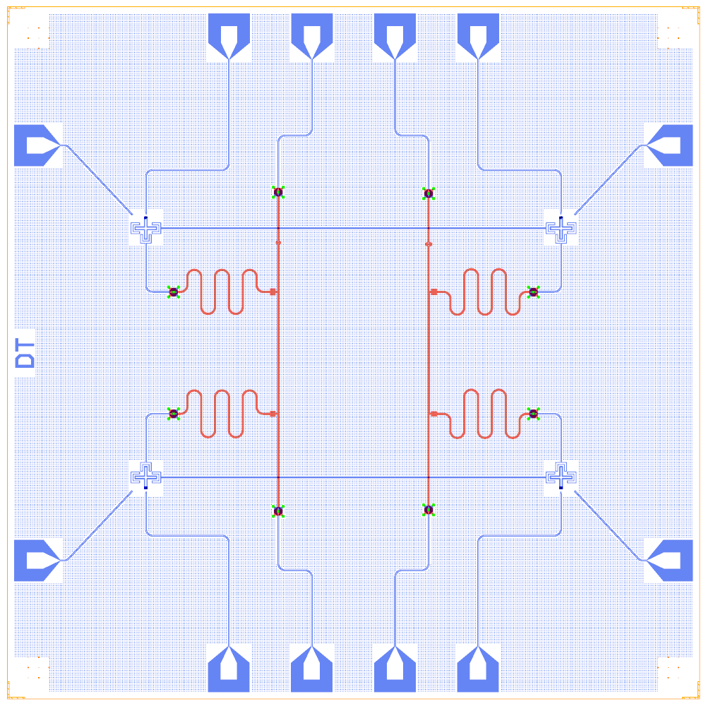
At a glance
Notebook |
|
Source |
KQCircuits |
Chip |
10 × 10 mm, two faces ( |
On the chip |
4 detuned Swissmons · 2 buses · 4 λ/2 readouts crossing to the top chip · 2 probe lines · 4 charge and 4 flux lines |
Builds today |
yes (layout built on 2026-11-19 in 11 s) |
How the notebook builds it
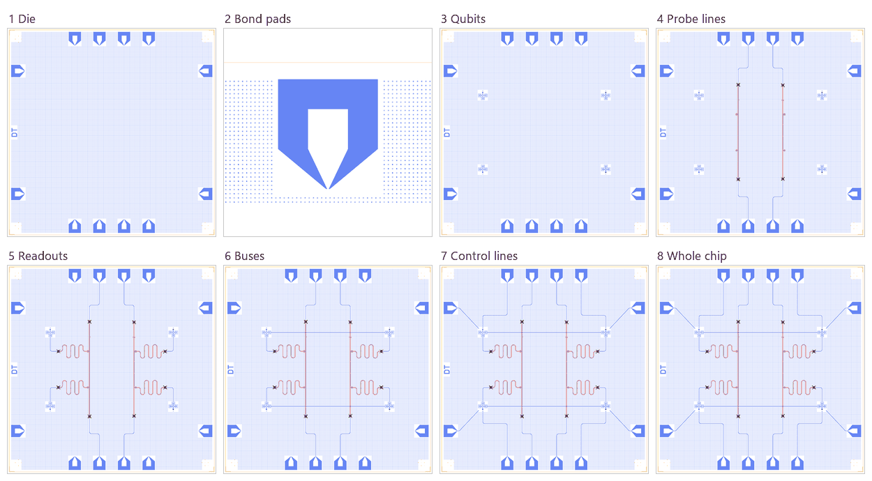
Die. The empty 10 × 10 mm chip with the Quantcore frame (dicing marks, alignment grids, chip boundary, device ID) and the ARD24 launchers.
Bond pads. The launchers moved so their outer etch edge sits 100 µm from the die edge (the pad rule).
Qubits. Four detuned Swissmons with Quantcore SQUIDs.
Probe lines. Top-chip readout capacitors and T’s, then the two probe lines.
Readouts. Four λ/2 resonators that change face to the top chip.
Buses. Two buses couple QB1 to QB2 and QB4 to QB3.
Control lines. Charge and flux lines from the launchers.
Whole chip. Sim groups, centring, design saved.
LOM estimates
Numbers are from a run of this notebook on 2026-11-19 (Setup, Design, Check and the LOM cells, 15 s): QuCat normal modes with QuTiP dressed values.
group |
qubit |
f_q (GHz) |
α (MHz) |
resonator |
f_r (GHz) |
κ (MHz) |
χ (MHz) |
|---|---|---|---|---|---|---|---|
QB1+RR1 |
QB1 |
6.012 |
-198 |
RR1 |
11.3 |
9.43 |
-0.122 |
QB3+RR3 |
QB3 |
5.81 |
-200 |
RR3 |
10.96 |
4.23 |
-0.121 |
QB2+RR2 |
QB2 |
5.913 |
-199 |
RR2 |
11.13 |
6.51 |
-0.122 |
QB4+RR4 |
QB4 |
5.705 |
-202 |
RR4 |
10.79 |
2.49 |
-0.12 |
group |
pair |
ZZ (kHz) |
neighbours |
hybridised |
|---|---|---|---|---|
QB1+QB2+CPL12 |
QB1-QB2 |
205 |
yes |
no |
QB3+QB4+CPL43 |
QB3-QB4 |
198 |
yes |
no |
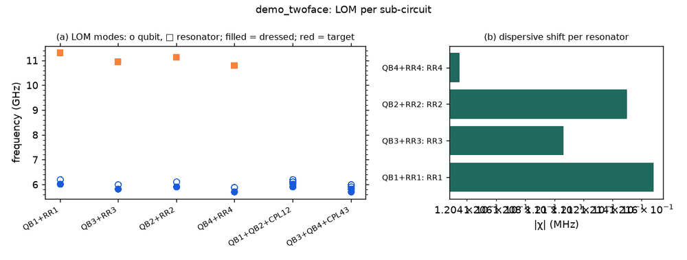
These are lumped-model estimates (component formulas and calibration), not FEM results; see the LOM page for how far to trust them.
Build spec
The rest of this page is the detailed spec the notebook was built from: every component, port, route and length.
Source other-libs/KQCircuits-main/KQCircuits-main/klayout_package/python/kqcircuits/chips/demo_twoface.py
(DemoTwoface, chip name “DT”), GPL-3.0 (IQM Finland). Rebuilt from extracted parameters. What it is: the
Demo topology split over two faces. The 4 Swissmons, 2 straight buses and all drive/flux lines are on the bottom chip
(face 0 = 1t1). Each readout resonator crosses to the top chip (face 1 = 2b1) through a flip-chip RF connector,
then meanders and couples (finger capacitor + T) to a probeline that runs on the top chip. 10 × 10 mm. The
top-chip box is (1500,1500)–(8500,8500) and the KQC frame = Designer frame. Flip-chip builds work.
Tested on 2026-11-02: chip={"frames_enabled": [0, 1]}, face_ids=["2b1","1t1"] on the top-chip cells and
Designer.waypoint(at, face_id="2b1") in routes. The build inserts FlipChipConnectorRf automatically, and the RR
length matches KQC. LOM, DRC and simulation are face-agnostic (see notes).
Components
instance |
catalog ref |
key params (units) |
at (x, y) |
rot |
notes |
|---|---|---|---|---|---|
QB1 |
|
|
(2000, 6800) |
0, |
cplr1 (2000,6581) S; cplr2 (2219,6800); drive (1800,7000); flux (2000,7045.33) N |
QB2 |
|
same |
(8000, 6800) |
180 |
cplr1 (8000,6581); cplr2 (7781,6800); drive (8200,7000) |
QB3 |
|
same |
(2000, 3200) |
0 |
cplr1 (2000,3419) N; cplr2 (2219,3200); drive (1800,3000); flux (2000,2954.67) |
QB4 |
|
same |
(8000, 3200) |
180, |
cplr1 (8000,3419); cplr2 (7781,3200); drive (8200,3000) |
C1–C4 |
|
|
(3836.5,5881) / (6163.5,5881) / (3836.5,4119) / (6163.5,4119) |
0 / 180 / 0 / 180 |
top chip |
PL1–PL4 |
|
|
snap |
(→ 270 / 90 / 270 / 90) |
top chip |
CIN1 / CIN2 |
|
|
(3914,6592) / (6086,6570) |
270 |
probeline input caps (top chip) |
Routes
route |
from → to |
type, length (µm) |
waypoints |
notes |
|---|---|---|---|---|
CPL12 / CPL43 |
QB1.cplr2 → QB2.cplr2 / QB4.cplr2 → QB3.cplr2 |
cpw a=4 b=9, 5562 each |
none (straight at y=6800 / 3200) |
bottom chip |
DL1–DL4 |
chip.DL-QBk → QBk.drive |
cpw |
(780,8000) / (9220,8000) / (780,2000) / (9220,2000) |
|
FL1–FL4 |
chip.FL-QBk → QBk.flux |
cpw 3388.83 |
QB1 (3200,7720),(2000,7720); QB2 (6800,7720),(8000,7720); QB3 (3200,2280),(2000,2280); QB4 (6800,2280),(8000,2280) |
|
RR1 |
QB1.cplr1 → C1.a |
meander=5000 |
(2000,5881), wp((2400,5881), face_id=”2b1”), (2500,5881) |
face change at 2400 inserts the FC connector; meander auto on (2500→3700) |
RR2 |
QB2.cplr1 → C2.a |
meander=5100 |
(8000,5881), wp((7600,5881), face_id=”2b1”), (7500,5881) |
|
RR3 |
QB3.cplr1 → C3.a |
meander=5200 |
(2000,4119), wp((2400,4119), face_id=”2b1”), (2500,4119) |
|
RR4 |
QB4.cplr1 → C4.a |
meander=5300 |
(8000,4119), wp((7600,4119), face_id=”2b1”), (7500,4119) |
KQC |
P1_in |
chip.PL-1-IN → CIN1.a |
cpw 2976.66 |
(4400,8220), (3914,8220), wp((3914,7323.5), face_id=”2b1”) |
|
P1_a / P1_b |
CIN1.b → PL1.left / PL1.right → PL3.left |
668.5 / 1740, |
none |
top chip |
P1_out |
chip.PL-1-OUT → PL3.right |
3708.16 |
(4400,1780), (3914,1780), wp((3914,2708), face_id=”2b1”) |
|
P2_in |
chip.PL-2-IN → CIN2.a |
2998.66 |
(5600,8220), (6086,8220), wp((6086,7301.5), face_id=”2b1”) |
|
P2_a / P2_b |
CIN2.b → PL2.right / PL2.left → PL4.right |
646.5 / 1740, |
none |
|
P2_out |
chip.PL-2-OUT → PL4.left |
3708.16 |
(5600,1780), (6086,1780), wp((6086,2730), face_id=”2b1”) |
L = {2: "FL-QB1", 3: "PL-1-IN", 4: "PL-2-IN", 5: "FL-QB2", 7: "DL-QB2", 12: "DL-QB4",
     14: "FL-QB4", 15: "PL-2-OUT", 16: "PL-1-OUT", 17: "FL-QB3", 19: "DL-QB3", 24: "DL-QB1"}
d = Designer("kqc_demo_twoface", launchers={"type": "ARD24", "assign": L}, chip={"name_chip": "DT", "frames_enabled": [0, 1]})
TOP = dict(face_ids=["2b1", "1t1"])
q1 = d.add("QB1", "Swissmon", at=(2000, 6800), mirror=True, junction=J, cpl_length=[120, 120, 120], port_width=[4, 10, 4])
c1 = d.add("C1", "FingerCapacitorSquare", at=(3836.5, 5881), finger_number=7, **TOP)
d.add("PL1", "WaveguideCoplanarSplitter", snap="bottom", to=c1.b, lengths=[11, 11, 41], port_names=["right", "left", "bottom"], **TOP)
d.route("RR1", q1.cplr1, c1.a, meander=5000, nodes=[(2000, 5881), Designer.waypoint((2400, 5881), face_id="2b1"), (2500, 5881)])
d.route("P1_b", "PL1.right", "PL3.left", face_ids=["2b1"])
Launchers, pads, test structures, markers, labels
ARD24 with KQC names (12 pads, bottom chip). N: FL-QB1 #2, PL-1-IN #3 (4400,9320), PL-2-IN #4 (5600,9320), FL-QB2 #5.
E: DL-QB2 #7, DL-QB4 #12. S: FL-QB4 #14, PL-2-OUT #15 (5600,680), PL-1-OUT #16 (4400,680), FL-QB3 #17. W: DL-QB3
#19, DL-QB1 #24. Both faces get chip frames (frames_enabled=[0,1]), and the RF connectors bring their own bump cells. There are
no junction tests.
LOM node structure (qubit ↔ resonator ↔ feedline ↔ bus ↔ control lines)
Same graph as demo, except: buses QB1–QB2 and QB4–QB3 only; probeline 1 serves QB1 and QB3, probeline 2 serves
QB2 and QB4. RRk are λ/2 at QBk.cplr1 (5.0–5.3 mm), with Ck as series C to the probeline nodes, and CINk are the
input series C. The cplr0 pads stay unconnected, as in KQC (tested full build: all KQC lengths reproduced, and only
QBk.cplr0 is unconnected). The LOM does not know faces. The bump connector is part of the RR route, and the capacitance to the
opposite chip face only comes from FEM. Run a C-matrix of the readout region with
both faces.
Targets (if stated)
None. readout_res_lengths as in Demo (5000–5300), include_couplers=True, junction_type = KQC default.
Simplifications for a first rebuild
Single-face fallback: drop all
face_idsandface_idwaypoints. You get a Demo variant with straight buses and probelines at x = 3914 / 6086.Then add the flip chip: frames_enabled, top-chip cells and face waypoints, as above.
Faces are pass-through parameters in Designer, not a schema feature. If DRC flags overlaps between faces, check whether it ignores faces.
Quantcore PDK rebuild
The notebook is a Quantcore-PDK rebuild of the source chip. The netlist, LOM and imported components are kept, and the process is Quantcore’s.
Notebook: examples/designs/kqc/demo_twoface.ipynb.
Chip: the Quantcore die frame (L dicing markers 1000/0, 3 × 3 alignment grids 1001/0, chip boundary 100/0, device ID where an edge is free; any brand text is QCT), drawn on the source’s 10 × 10 mm chip (its launchers sit on the chip edges, so the design does not fit the 7.5 mm die). KQC’s ChipFrame (dicing edge, corner markers, labels) is not drawn. KQC’s original grids its whole ground plane (
with_grid, 5 µm squares on a 10 µm step). The rebuild keeps that coverage at the PDK density instead (chip parametercheese: "chip",with_grid: false): 5 µm squares with 20 µm gaps over the whole die, at least 4 µm from the 3/0 keep-outs, inside the design area and clear of the frame markers and the device ID. The top chip (face 2b1) gets no frame, because PDK v3 defines none for the flip-chip top chip (its layers export to 800–804/0).Stack: sapphire 650 µm, εr 10.25 (the PDK default stack, used by the LOM estimates and every FEM export); KQC’s own simulation default is silicon (εr 11.45), so LOM capacitances and resonator frequencies here are for sapphire.
Junctions: Quantcore Nb/AlOx/Nb trilayer junctions (
junction_typefromlayouts.registry.trilayer_junction): fingers on 2/0 + 4/0, spacer 50/0 with the 51–53/0 gradient, sized on the PDK junction rule (Nb Δ = 1.4 meV, I_c·R_n = πΔ/2e, R_n·A 13.5 kΩ·µm² and C_J 50 fF/µm² assumed); every Swissmon’s SQUID becomes a Quantcore SQUID (KQC’sjunction_widthsets the straight finger, bent finger 0.6 µm), detuned by finger width so the bus-coupled pairs do not hybridise: 0.27 / 0.26 / 0.25 / 0.24 µm → R_n 41.7 / 43.3 / 45.0 / 46.9 kΩ (all in the 40–50 kΩ window), L_J 6.24 / 6.48 / 6.73 / 7.02 nH, C_J ≈ 15 fF, in place of the assumed 15–18 nH + 2 fF. Expected f_q ≈ 6.0 / 5.9 / 5.8 / 5.7 GHz (estimates; were 4.07 … 3.70 GHz).Kept: the topology and every KQC element with the source’s parameters, positions and orientations, the launcher assignment, every route’s path and length, the sim groups (both faces, the face changes and flip-chip connectors, readouts 5000–5300 µm).