Floating transmon (SQDMetal)
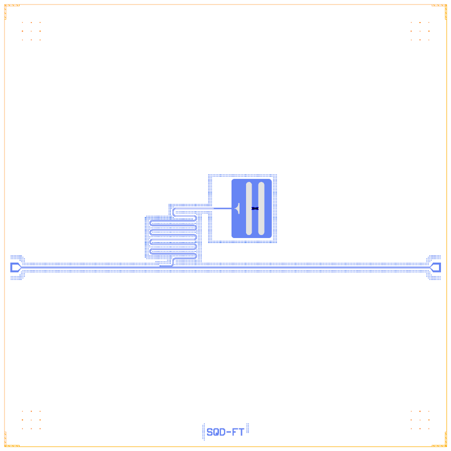
One floating tapered-inset transmon with a λ/2 readout that ends in a coupled section on a short through line. It is SQDMetal’s Palace eigenmode example (Apache-2.0), rebuilt on the Quantcore PDK. The source’s open line ends become two small bond pads, because the LOM needs real ports.
Build this one to learn a λ/2 readout on a through line and the Quantcore TransmonTaperedInsets cell.
At a glance
Notebook |
|
Source |
SQDMetal example |
Chip |
7.5 × 7.5 mm Quantcore die, the source’s 4 × 4 mm area in its middle, CPW 10 / 6 µm |
On the chip |
2 bond pads · 1 line · 1 tapered-inset transmon · 1 λ/2 readout (8960 µm) |
Builds today |
yes (layout built on 2026-11-19 in 8 s) |
How the notebook builds it
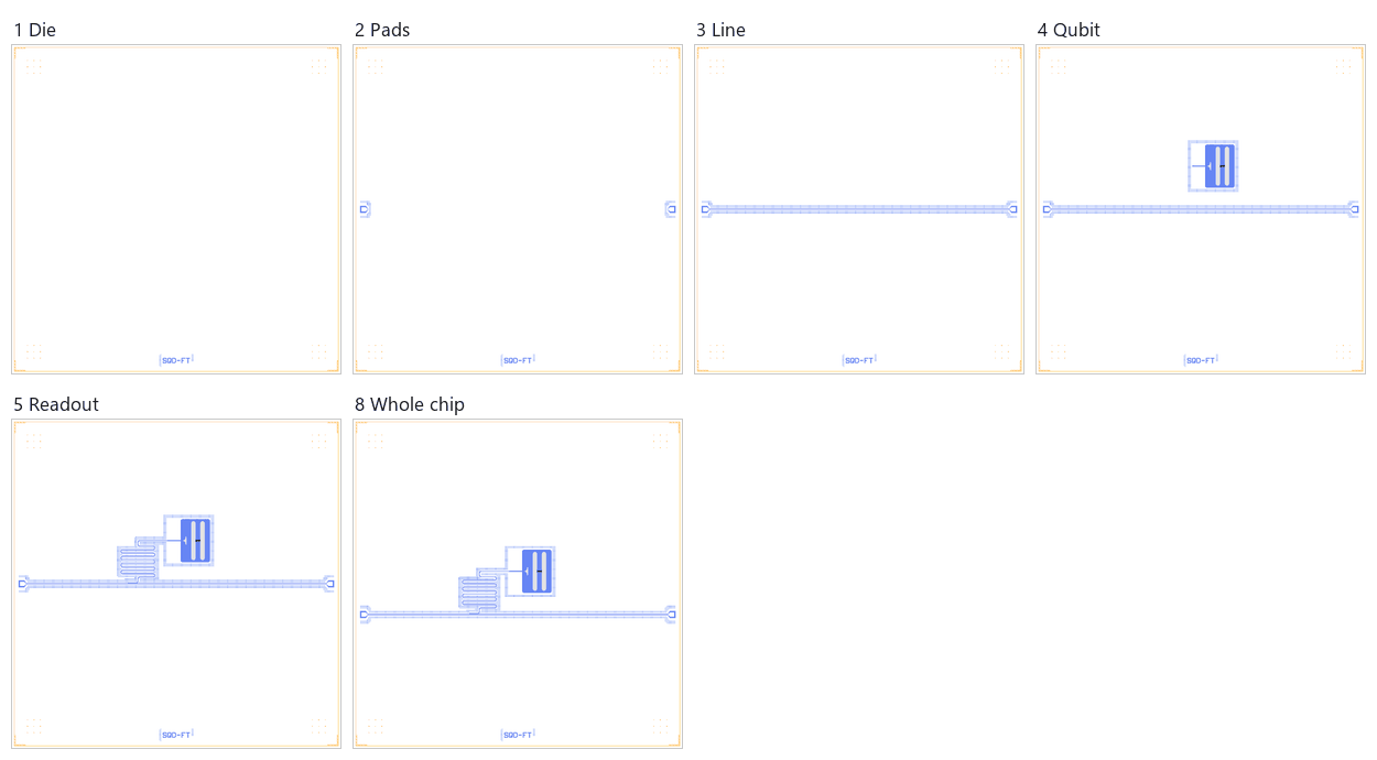
Die. The Quantcore die with the frame and the device ID.
Bond pads. Two small pads that replace the source’s open line ends.
Line. A straight 10 / 6 µm through line between the pads.
Qubit. One
TransmonTaperedInsetswith the source’s options.Readout. The λ/2 meander from the qubit to the coupled section on the line.
Coupling. None: one qubit.
Control lines. None.
Whole chip. Targets (f_q 4.5 GHz, f_r 6.8 GHz), one sim group, centring, save.
LOM estimates
Numbers are from a run of this notebook on 2026-11-19 (Setup, Design, Check and the LOM cells, 8 s): QuCat normal modes with QuTiP dressed values.
mode |
kind |
f (GHz) |
κ (MHz) |
A (MHz) |
participation |
|---|---|---|---|---|---|
Q1 |
qubit |
4.676 |
0 |
181 |
J_Q1 1.00 |
R1 |
resonator |
6.907 |
0.00792 |
0 |
R1 1.00 |
parameter |
LOM (QuTiP) |
target |
|---|---|---|
|
4.49 |
4.5 |
|
-201 |
– |
|
-0.411 |
– |
|
6.91 |
6.8 |
|
0.00792 |
– |
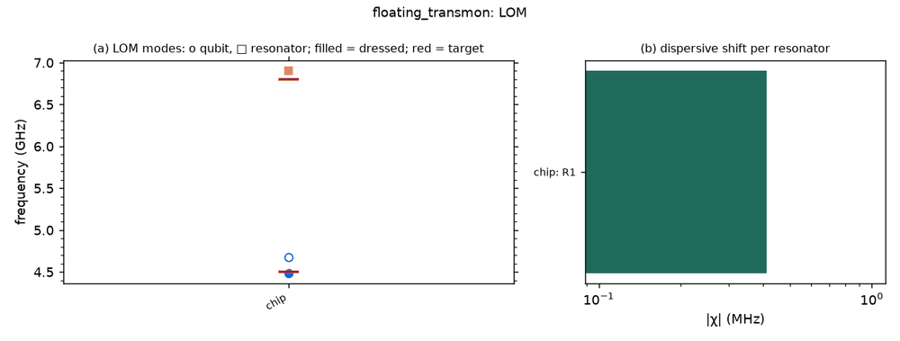
These are lumped-model estimates from component formulas and calibration, not FEM results. The LOM page says how far to trust them.
Build spec
The rest of this page is the detailed spec the notebook was built from: every component, port, route and length.
The KQC
DoublePadsstand-in has a LOM model. The Quantcore rebuild usesTransmonTaperedInsets.
Source: doc-sphinx/source/examples/Palace_Eigenmode_FloatingTransmon.ipynb
· SQDMetal TransmonTaperedInsets + Quantum Metal CoupledLineTee, RouteMeander, RouteStraight, OpenToGround ·
licence Apache-2.0 (verified) · read on 2026-11-02. No stored outputs. Exports GDS via MakeGDS(...).export(positive),
then runs a Palace capacitance / eigenmode setup (3 modes from 3 GHz).
What it is: one floating tapered-pad transmon. Its readout connector pad runs a λ/2 meander to a CoupledLineTee
with an open termination, hung on a short straight transmission-line segment (both ends OpenToGround; the
simulation adds 50 Ω ports).
Frame: chip 4 × 4 mm centred at (0, 0), substrate 500 µm, silicon (siliconcryo). Box (0, 0, 4000, 4000),
Designer = source + (2000, 2000). CPW width 10 µm, gap from CpwParams.get_gap_from_width for 50 Ω on Si
(≈ 6 µm, not printed).
TransmonTaperedInsets has no KQC equivalent. A DoublePads stand-in covers it for a first build.
Components
instance |
catalog ref |
key params (units) |
at (x, y) Designer |
rot |
notes |
|---|---|---|---|---|---|
Q1 |
|
defaults: pads 800 × 110, pocket 1000 × 800, taper_height 0 (override), pad_gap 100, inductor_height 100. Readout connector pad_gap 100 (pad 200 × 30, cpw_extend 200) |
(2500, 3000) |
90 (dipole along +x) |
source (0.5, 1.0) mm |
T1 |
coupled section (Metal |
coupling_length 220, coupling_space 5 (ground strip), down_length 100, open_termination True |
centre (1000, 2000) |
180 |
source (−1.0, 0) mm |
P_L / P_R |
|
(≈100, 2000) / (≈3900, 2000) |
270 / 90 |
source line spans x −1.8…0 mm. Extend it to pads |
Junction: not given; target f_q 4.5 GHz. Assume junction={"Lj_nH": 14, "Cj_fF": 0} (E_C ≈ 0.2 GHz, assumed).
Routes
route |
from → to |
type, length |
hanger |
notes |
|---|---|---|---|---|
FL |
P_L.a → P_R.a |
cpw 10/6 |
straight y 2000 |
source |
R1 |
Q1.cplr → FL.hanger |
meander 8960 total (λ/2 at 6.8 GHz incl. CLT and connector wire; the meander alone is 8960 − extras) |
s at x 1000 (s = 1000 − x(P_L.a)), length 220, side left (resonator above FL), ground_gap 5, end=”open” |
meander spacing 100, fillet 40, leads 125/125, asymmetry 0 |
L_halfwave = 8.96 mm (the same calculation is printed as 8.96 mm in 2_transmons_wres_comp).
Launchers, pads, test structures, markers, labels
None in the source. Add pads only for a fab version.
LOM node structure
Q1: floating two-island transmon with JJ. The readout pad couples by C_g to one island and starts R1 (λ/2, open at both ends, 6.8 GHz). R1’s far open end couples to FL over 220 µm with a 5 µm ground strip. FL: two 50 Ω ports.
Targets (stated)
f_q 4.5 GHz, f_res 6.8 GHz (λ/2).
Simplifications for a first rebuild
DoublePads stand-in (island extents [800, 110], island_island_gap 100, ground_gap [1000, 800]) with
cplrtoward +y after rotation.Our hanger ends
open, so R1 is a native route. Check that the λ/2 length (not λ/4) is what the LOM bridge assumes for an open-open route.
Build with the stand-in
The stand-in build uses the DoublePads stand-in (pads 800 × 110, gap 100, pocket 1000 × 800, rot 90, 200 × 30 coupler); line between two 100 µm BondPads at the source open ends; open hanger 220 µm / 5 µm, backward (open at the west end); Lj 14 nH assumed.
Rebuild with TransmonTaperedInsets
The DoublePads stand-in is replaced by TransmonTaperedInsets with the source options (connection_pads readout pad_gap
100, inductor_height 100, pad_gap 100, taper_height 0, rot 90). R1 starts at the cell’s readout pin (700 µm from the
centre, as SQDMetal); the 410 µm connector wire is inside the cell, so the route is 8960 − 410 = 8550 µm. LOM (Lj 14 nH
assumed; pads analytic 93 / 106 / 44 fF; connection pad + wire 73 fF to gnd): f_q 4.10 GHz (target 4.5), α −225 MHz,
λ/2 7.02 GHz (target 6.8 on Si), χ −0.36 MHz, κ 0.0066 MHz (with the stand-in: 4.46 GHz / 7.01 GHz / χ −0.59).
Open issue: the drawn Manhattan junction does not bridge the 100 µm gap (components).
Quantcore PDK rebuild
The notebook is a Quantcore PDK rebuild of the source, not a replica: the netlist, LOM and imported components are kept, and the process is Quantcore’s.
Notebook: examples/designs/sqdmetal/floating_transmon.ipynb.
Chip: the Quantcore die frame (L dicing markers 1000/0, 3 × 3 alignment grids 1001/0, chip boundary 100/0, device ID where an edge is free; any brand text is QCT), on the 7.5 × 7.5 mm Quantcore die; the source’s 4 × 4 mm chip area is centred in it (
box=(-1750, -1750, 5750, 5750)), so every coordinate stays the source’s.Stack: sapphire 650 µm, εr 10.25 (the PDK default stack, used by the LOM estimates and every FEM export); the SQDMetal examples are on silicon (280–500 µm), so frequencies differ from the source’s.
Junctions: Quantcore Nb/AlOx/Nb trilayer junctions (
junction_typefromlayouts.registry.trilayer_junction): fingers on 2/0 + 4/0, spacer 50/0 with the 51–53/0 gradient, sized on the PDK junction rule (Nb Δ = 1.4 meV, I_c·R_n = πΔ/2e, R_n·A 13.5 kΩ·µm² and C_J 50 fF/µm² assumed). The junction is sized for the source’s target f_q 4.5 GHz with the LOM C_Σ ≈ 98 fF: straight finger 0.31 µm × 0.6 µm, L_J ≈ 10.9 nH, C_J ≈ 9.3 fF, so R_n ≈ 72 kΩ, above the 40–50 kΩ window (a 45 kΩ junction would put it at ≈ 5.6 GHz). It is drawn across the 100 µm pad gap byTransmonTaperedInsets(junction_params); cell 1 prints the sizing.Kept: the topology and the components with the source’s options and positions, the 8960 µm λ/2 readout, the 220 µm / 5 µm coupled section, the targets, the sim group.