iSWAP 1: concentric transmons
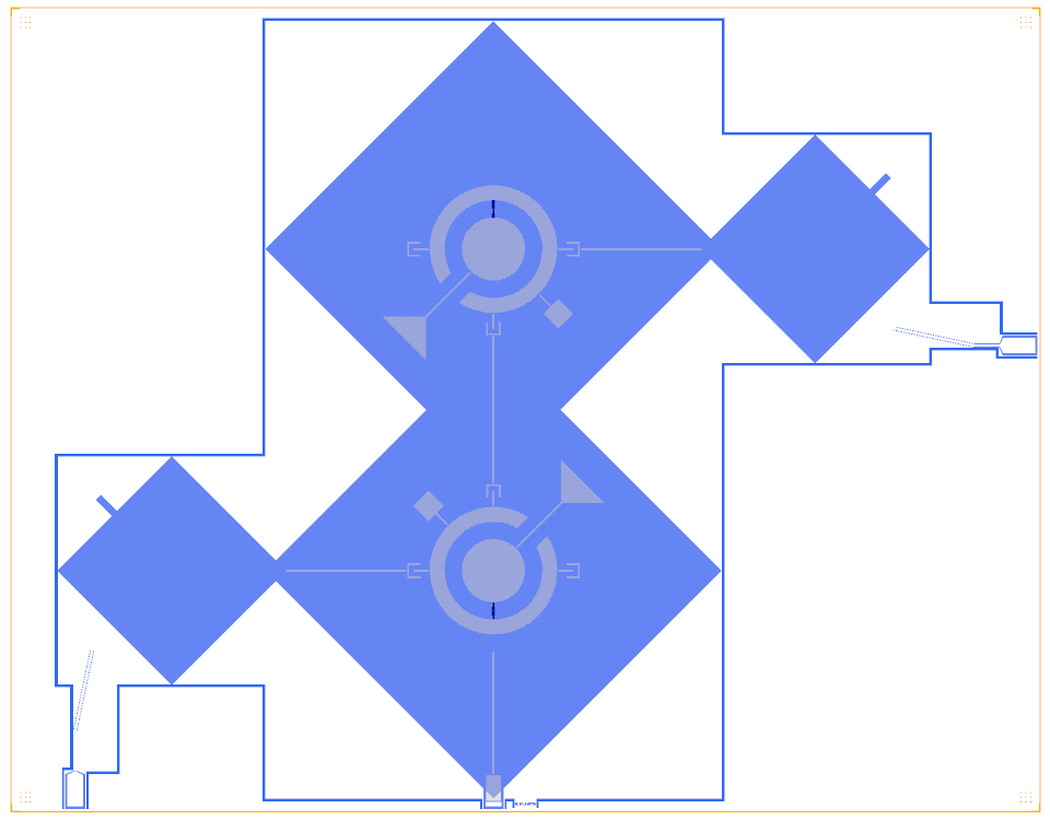
Two mm-scale concentric transmons (a disk inside a SQUID ring) coupled directly by a straight 4.6 mm line, each wired to a lumped meander resonator, with a separate drive line. It is example 1 of the Qiskit Metal iSWAP-gate notebook (after Phys. Rev. Applied 10, 034050; Apache-2.0, © IBM and contributors). The notebook says the aim is to show the structure of each device, and that the exact geometry is secondary. The Quantcore rebuild is distributed under GPL-3.0.
Build this one to learn how large metal-frame components (lumped resonators, concentric qubits) sit in pockets, and how lines inside a pocket are drawn as metal strips with a wire.
At a glance
Notebook |
|
Source |
Qiskit Metal |
Chip |
32 × 25 mm (the pockets overhang the source’s 32 × 20 mm chip) |
On the chip |
2 concentric transmons with Quantcore SQUIDs · 2 lumped resonators (5 × 5 mm frame) · 1 direct 4.6 mm coupling line · 1 drive line · 3 bond pads |
Builds today |
yes (layout built on 2026-11-19 in 12 s) |
How the notebook builds it
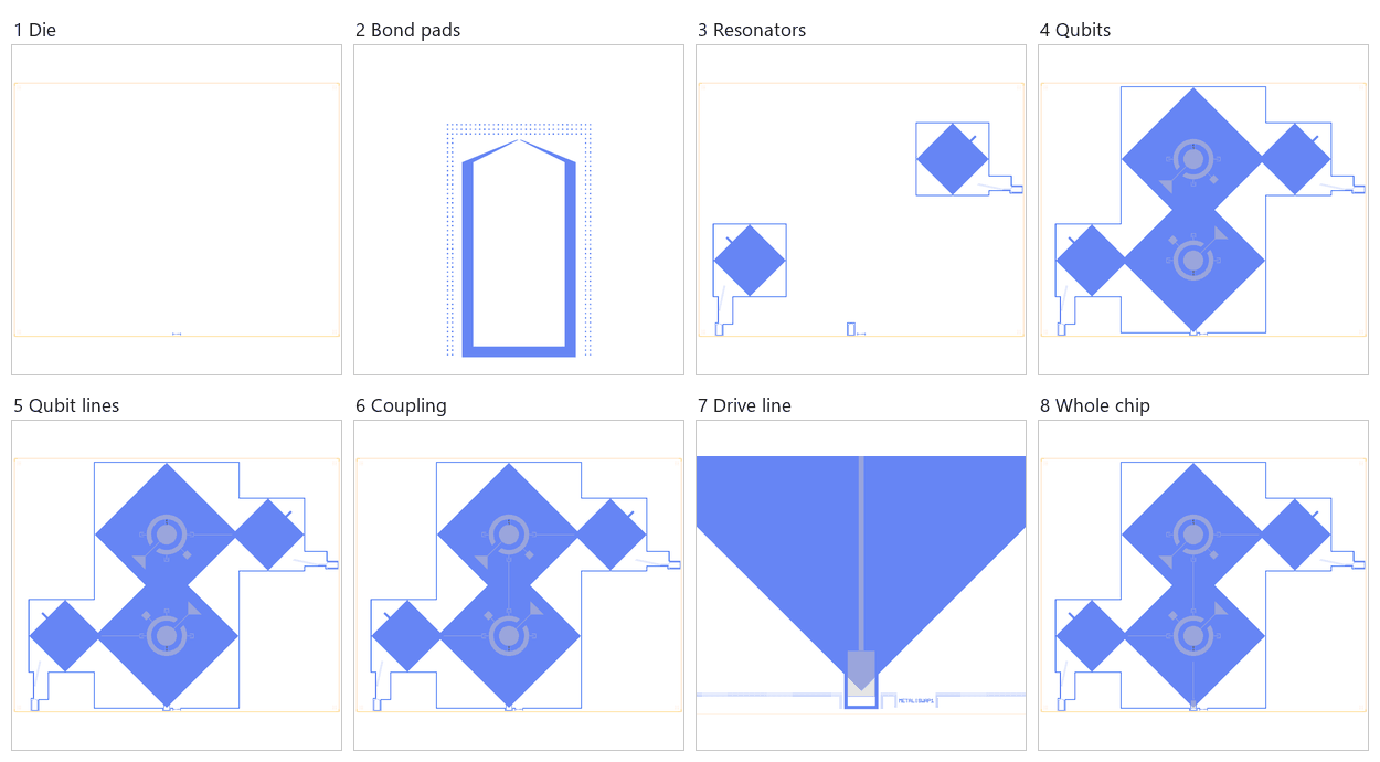
Die. An empty 32 × 25 mm chip with the QCT frame (dicing marks, alignment grids, chip boundary, device ID).
Bond pads. Three launchpads slid to the 100 µm pad-edge rule (the picture zooms on one pad).
Resonators. Two lumped resonators with their pockets and lines to the pads.
Qubits. Two concentric transmons with Quantcore SQUIDs, at -45° and 135°, with their pockets.
Qubit lines. The lines from the qubits’
pin3fingers to the resonators.Coupling. The straight 4.6 mm line between the two qubits.
Drive line. An open-ended line that ends 500 µm below qubit 1’s ring (the picture zooms on it).
Whole chip. The sim group for the qubits, the centring check, the design saved.
LOM estimates
Numbers are from a run of this notebook on 2026-11-19 (Setup, Design, Check and the LOM cells, 10 s): QuCat normal modes with QuTiP dressed values.
group |
pair |
ZZ (kHz) |
neighbours |
hybridised |
|---|---|---|---|---|
qubit1+route1+qubit2 |
qubit1-qubit2 |
– |
yes |
yes |
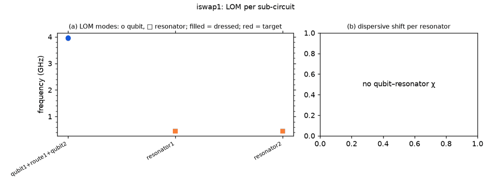
These are lumped-model estimates from component formulas and calibration, not FEM results. The LOM page says how far to trust them.
Build spec
The rest of this page is the detailed spec the notebook was built from: every component, port, route and length.
The
metal:references in this spec build as written, through themetal:wrapper (ports are the Metal pin names, parameters the Metal options). The Quantcore and KQC substitutions are optional.
The notebook
examples/designs/metal/iswap1_concentric_direct.ipynbbuilds allmetal:cells at the source’s scale. Pockets Metal never draws are added asmetal:Rectangle subtract(qubits 10 × 10 mm, resonators inside the frame plus a slot), in-pocket lines are metal traces plus wires, and the chip is 32 × 25 mm.
Source: Quantum Metal docs/circuit-examples/F.Small-quantum-chips/Full-Physical-Design-of-iSWAP-Gates.ipynb,
Example 1. Licence Apache-2.0. It follows Phys. Rev. Applied 10, 034050 (2018) “only roughly”; the notebook says “the
point is the structure of each device, not its exact geometry”.
Two TransmonConcentricType2 qubits at 45° are joined directly by a straight CPW. Each qubit drives a lumped
(spiral) readout resonator ResonatorLumped that goes to a pad. A third pad carries a drive line that ends open near
qubit 1.
Everything is mm-scale: qubit rad_outer 2 mm, pocket 10 × 10 mm, resonator box 5 × 5 mm, cpw_width set to
0.1 mm (gap 6 µm default), pads 0.5 × 1 mm. The chip is 32 × 20 mm, centred at (1, 3) mm, so
Designer = Metal + (15000, 7000). Metal layer 1, silicon default.
A topology-only rebuild uses these substitutions: KQC ConcentricTransmon for
TransmonConcentricType2, KQC SpiralResonatorPolygon for ResonatorLumped, BondPad.
Components
instance |
catalog ref |
key params (Metal) |
at (x, y) |
rot |
notes |
|---|---|---|---|---|---|
qubit1 |
|
rad_outer 2 mm, rad_inner 1 mm, gap 0.5 mm, jj_w 0.2 mm, pocket 10 mm, fingers 0.1 × 0.5 mm, N finger 2 mm |
(15000, 7000) |
Metal −45 |
Metal pins (Designer frame): pin1 (17700, 7000) E, pin2 (15000, 9700) N, pin3 (12300, 7000) W |
qubit2 |
|
same |
(15000, 17000) |
Metal 135 |
pin1 (12300, 17000) W, pin2 (15000, 14300) S, pin3 (17700, 17000) E |
resonator1 |
|
box 5 × 5 mm, res_width 10 µm, 14 turns, turn_radius 0.1 mm, inner/outer space 0.19/0.1 mm |
(25000, 17000) |
Metal −45 |
pins used: pin_sw (21464.5, 17000) W, pin_east (26767.8, 15232.2) at −45° |
resonator2 |
|
same |
(5000, 7000) |
Metal 45 |
pins used: pin_se (8535.5, 7000) E, pin_west (3232.2, 5232.2) at −135° |
P1_C, P2_C, P3_C |
|
lead_length 0 |
(15000, 2000), (2000, 2000), (30000, 14000) |
0, 0, 90 |
P3 faces W |
open1i |
free end (metal:OpenToGround) |
width 100 (cpw_width var), gap 6 |
(15000, 4500) |
— |
drive line end, 2.5 mm below qubit1 |
Routes
route |
from → to |
type, length |
waypoints |
notes |
|---|---|---|---|---|
route1 |
qubit1.pin2 → qubit2.pin2 |
cpw 4600 |
— |
direct qubit–qubit coupling line (straight, N–S) |
route2 |
resonator1.pin_sw → qubit2.pin3 |
cpw 3764 |
— |
readout coupling |
route3 |
resonator2.pin_se → qubit1.pin3 |
cpw 3764 |
— |
|
route4 |
resonator1.pin_east → P3_C.a |
cpw 3580 |
[(27475, 14525), (29950, 14000)] |
start lead 1 mm |
route5 |
resonator2.pin_west → P2_C.a |
cpw 3580 |
[(2525, 4525), (2000, 2050)] |
start lead 1 mm |
route6 |
P1_C.a → |
cpw 2500 |
— |
drive line to qubit1 |
All Metal routes are RouteStraight with zero leads unless stated. Trace 100 µm; Metal’s gap stays 6 µm.
Launchers, pads, test structures, markers, labels
3 pads: P1 (drive), P2 (resonator2 out), P3 (resonator1 out). There are no markers.
LOM node structure
qubit1 (fixed) and qubit2 (flux-tunable in the paper; no flux line is drawn) are each a concentric island pair with a JJ.
A direct coupling network (route1) joins the two pin2 couplers: C_g1–line–C_g2.
Each qubit couples (pin3) to a lumped LC resonator, which is galvanically connected to a 50 Ω port.
P1 is an open drive line (C_d to qubit1).
Targets (if stated)
None (no LOM or simulation for this example).
Simplifications for a first rebuild
Rebuild at µm scale (divide all sizes and positions by about 10; chip 3.2 × 2 mm) with the KQC defaults for ConcentricTransmon (coupler_1/2/3, drive ports) and SpiralResonatorPolygon (ports a, b). Use it only as a reference for anything quantitative.
Map the pins: qubit pin2 →
coupler_2, pin3 →coupler_3, drive →drive. Resonator in/out → a/b.
Quantcore PDK rebuild
The notebook is a Quantcore PDK rebuild of the source, not a replica: the netlist, LOM and imported components are kept, and the process is Quantcore’s.
Notebook: examples/designs/metal/iswap1_concentric_direct.ipynb.
Chip: the Quantcore die frame (L dicing markers 1000/0, 3 × 3 alignment grids 1001/0, chip boundary 100/0, device ID where an edge is free; any brand text is QCT), drawn on the source’s 32 × 25 mm chip (the design does not fit the 7.5 mm die); no KQC chip frame.
Stack: sapphire 650 µm, εr 10.25 (the PDK default stack, used by the LOM estimates and every FEM export); Metal’s
DesignPlanardefault is silicon (εr 11.45, 750 µm), so the LOM capacitances, resonator frequencies and FEM jobs here are for sapphire rather than the source’s substrate.Junctions: Quantcore Nb/AlOx/Nb trilayer junctions (
junction_typefromlayouts.registry.trilayer_junction): fingers on 2/0 + 4/0, spacer 50/0 with the 51–53/0 gradient, sized on the PDK junction rule (Nb Δ = 1.4 meV, I_c·R_n = πΔ/2e, R_n·A 13.5 kΩ·µm² and C_J 50 fF/µm² assumed); both qubits get a Quantcore SQUID (the source’s are SQUIDs) sized for 4.0 GHz, the bottom of the PDK band: the mm-scale islands (C_Σ ≈ 0.8 pF) would sit at ≈ 2.1 GHz with the nominal SQUID. Straight fingers 0.91 µm × 0.6 µm per junction, L_J 1.85 nH in parallel, C_J 55 fF, so R_n ≈ 12 kΩ, far below the 40–50 kΩ window. This geometry is incompatible with the PDK window at 4–8 GHz (flagged). The two qubits stay identical.Kept: the topology and every Metal component with the source’s options (through the
metal:wrapper), positions and orientations, every route’s end pins and total length, the sim groups (including the pockets Metal never draws, which the rebuild adds).