KQC test chips
These are KQCircuits’ own test structures: chips that test a process or a part rather than a quantum device. Two of them (simple, shaping) carry a qubit. The rest test airbridges, junctions, lithography, flip-chip crossings, through-silicon vias and the sample holder. All are 10 × 10 mm and rebuilt on the Quantcore PDK (GPL-3.0, © IQM Finland Oy).
Build them to see how a whole KQC chip cell is placed in a Designer and what each process test looks like. Each block below has the whole chip, a one-line purpose and how the notebook builds it. Most have no qubit or resonator, so their LOM section has nothing to estimate.
The notebooks
Notebook |
What it tests |
|---|---|
|
a minimal connected chip: one Swissmon coupled to a through line; the smoke test for KQC parity |
|
a readout design: one Swissmon with two Purcell-filtered quarter-wave readout chains |
|
airbridge crossings of lines, and a mechanical array of 608 short bridge spans (19 lengths, 8 widths, 4 distances) |
|
four-point DC resistance of airbridge chains (1 to 22 bridges per test) |
|
flip-chip line crossings (bridges on the top chip) and a crosstalk pair |
|
resonator quality factor with a flip-chip lid: six capped spiral quarter-wave resonators on one probe line |
|
a 40-pad sample holder: every pad pair is joined by a line |
|
electron-beam lithography with the ground removed in a cross-shaped area |
|
electron-beam lithography and junction process: a cross opening filled with an array of 80 × 80 µm squares |
|
SQUID junction arrays on test pads, with stepped junction widths |
|
optical lithography resolution: stripe blocks with 1 to 15 µm lines, spaced 1 and 5 times the width, and crosses |
|
the same lithography test on both faces of a flip chip |
|
ground-grid and lithography stripes: 80 µm metal stripes at 200 µm pitch and 80 µm squares in a cross opening |
|
the through-silicon-via process: a TSV fence pattern and three metrology arrays for cross-sections |
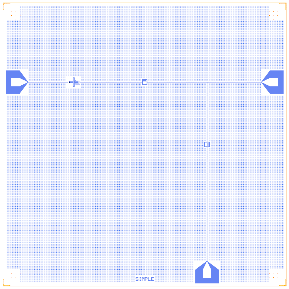
simple
Tests: a minimal connected chip: one Swissmon coupled to a through line; the smoke test for KQC parity.
Notebook |
|
Source |
KQCircuits |
On the chip |
3 SMA8 launchers (WN, EN, SE) · 1 Swissmon · 2 finger capacitors · 1 T · 1 flux line |
Builds today |
yes (layout built on 2026-11-19 in 7 s) |
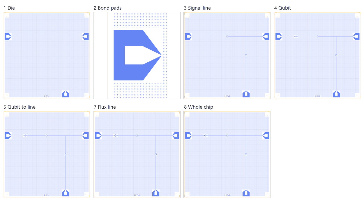
How it builds: Die, bond pads, signal line, qubit, qubit onto the line, flux line, whole chip.
Numbers are from a run of this notebook on 2026-11-19 (Setup, Design, Check and the LOM cells, 7 s): QuCat normal modes with QuTiP dressed values.
mode |
kind |
f (GHz) |
κ (MHz) |
A (MHz) |
participation |
|---|---|---|---|---|---|
QB |
qubit |
6.193 |
0.425 |
198 |
J_QB 1.00 |
parameter |
LOM (QuTiP) |
target |
|---|---|---|
|
5.99 |
– |
|
-214 |
– |
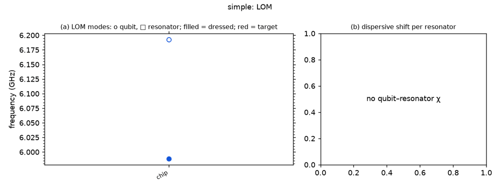
These are lumped-model estimates (component formulas and calibration), not FEM results; see the LOM page for how far to trust them.
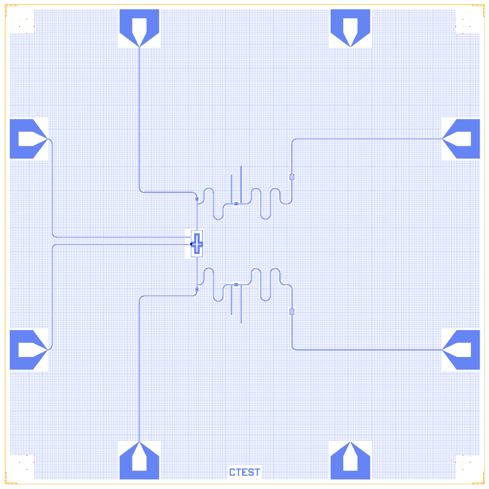
shaping
Tests: a readout design: one Swissmon with two Purcell-filtered quarter-wave readout chains.
Notebook |
|
Source |
KQCircuits |
On the chip |
8 SMA8 launchers · 1 Swissmon · 2 readout chains (resonator, filter, capacitors) · charge and flux line |
Builds today |
yes (layout built on 2026-11-19 in 7 s) |
How it builds: Die, bond pads, qubit, the two chains, control lines, whole chip.
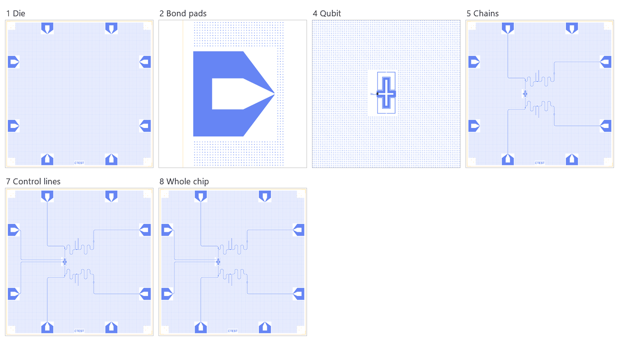
Numbers are from a run of this notebook on 2026-11-19 (Setup, Design, Check and the LOM cells, 17 s): QuCat normal modes with QuTiP dressed values.
parameter |
LOM (QuTiP) |
target |
|---|---|---|
|
6.45 |
– |
|
-242 |
– |
|
-0.00569 |
– |
|
-0.00847 |
– |
|
7.48 |
– |
|
27.5 |
– |
|
7.72 |
– |
|
27.9 |
– |
qubit |
f_q (GHz) |
A (MHz) |
resonator |
f_r (GHz) |
κ_r (MHz) |
χ (MHz) |
|---|---|---|---|---|---|---|
QB |
6.68 |
222 |
RA3 |
8.345 |
0.326 |
-6.46 |
resonator |
LOM line (µm) |
KQC target sum (µm) |
T arms not in the LOM (µm) |
|---|---|---|---|
RA3 |
2750 |
3060 |
306 |
PA2 |
3790 |
3950 |
153 |
RB3 |
2870 |
3170 |
306 |
PB2 |
3910 |
4070 |
153 |
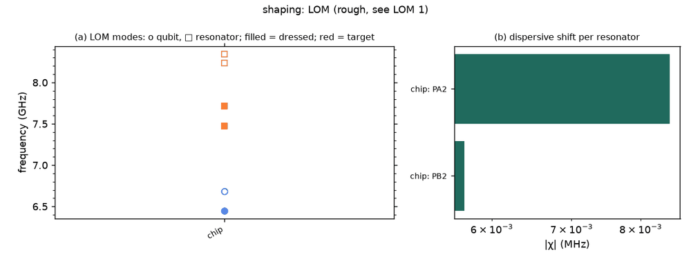
These are lumped-model estimates (component formulas and calibration), not FEM results; see the LOM page for how far to trust them.
airbridge_crossings
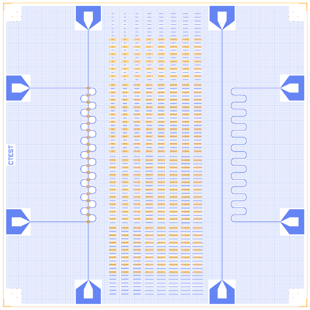
Tests: airbridge crossings of lines, and a mechanical array of 608 short bridge spans (19 lengths, 8 widths, 4 distances).
Notebook |
|
Source |
KQCircuits |
On the chip |
4 lines (PL-1 to PL-4) between SMA8 launchers · line crossings on airbridges · the mechanical array |
Builds today |
yes (layout built on 2026-11-19 in 73 s) |
How it builds: Die, bond pads, the mechanical array, the four lines.
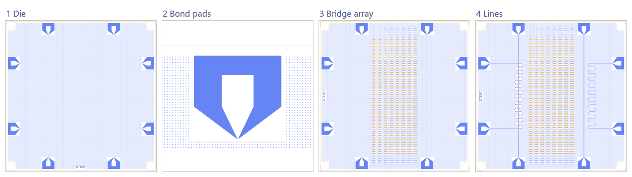
This chip has no junction or resonator (four 50 Ω through lines), so there is no lumped-model estimate. What it measures (the transmission across the crossings and the PL-1 to PL-3 crosstalk) needs a driven FEM solve.
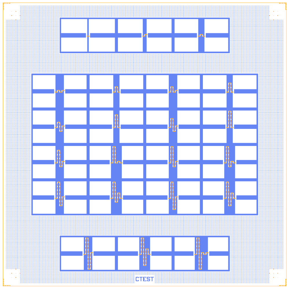
airbridge_dc_test
Tests: four-point DC resistance of airbridge chains (1 to 22 bridges per test).
Notebook |
|
Source |
KQCircuits |
On the chip |
22 |
Builds today |
yes (layout built on 2026-11-19 in 4 s) |
How it builds: Die, the chip cell, a view of the longest chain.
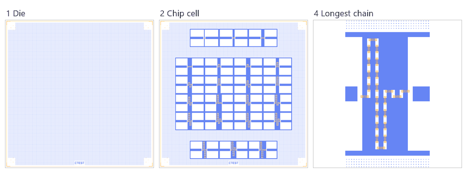
This chip has no junction, qubit or resonator, so there is no lumped-model estimate, and the notebook’s LOM section says there is nothing to simulate. The chip is measured in the process (optical or EBL inspection, DC probing) and not with microwaves.
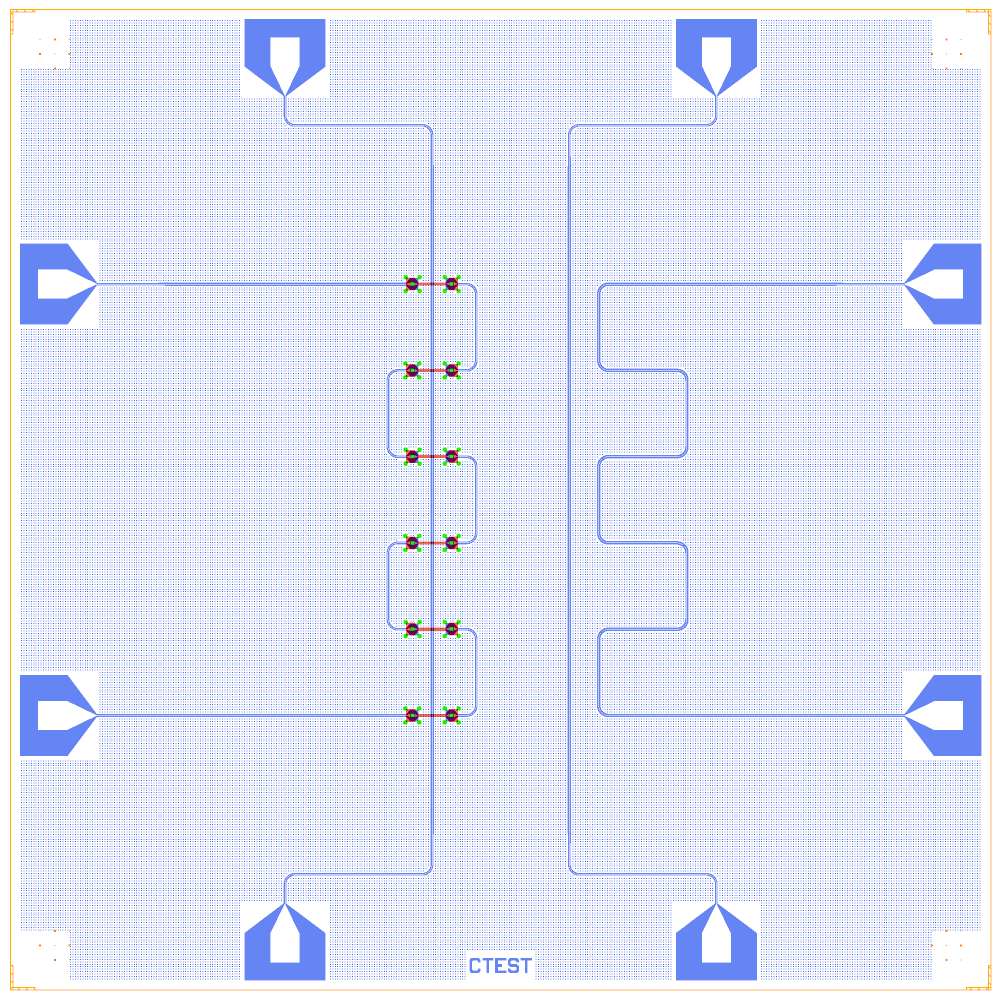
crossing_twoface
Tests: flip-chip line crossings (bridges on the top chip) and a crosstalk pair.
Notebook |
|
Source |
KQCircuits |
On the chip |
4 routes between SMA8 launchers · 6 flip-chip crossings of PL-1 by PL-3 |
Builds today |
yes (layout built on 2026-11-19 in 5 s) |
How it builds: Die, bond pads, the two straight lines, the crossing lines.
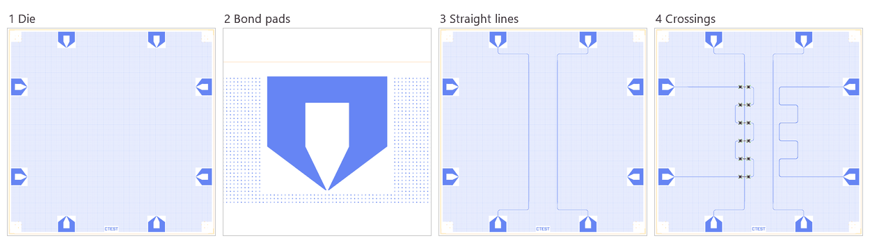
This chip has no junction or resonator (four 50 Ω through lines), so there is no lumped-model estimate. What it measures (the transmission through the flip-chip crossings and the PL-1 to PL-3 and PL-2 to PL-4 crosstalk) needs a driven FEM solve.
quality_factor_twoface
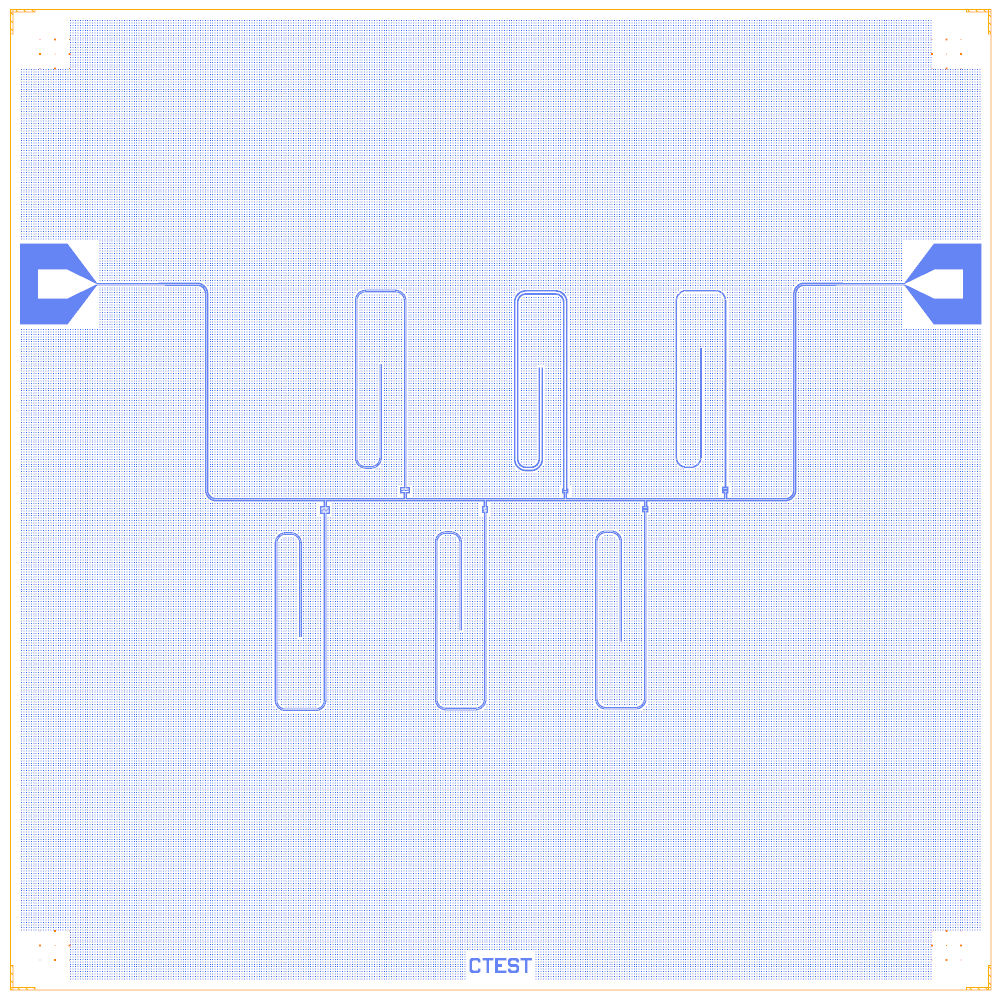
Tests: resonator quality factor with a flip-chip lid: six capped spiral quarter-wave resonators on one probe line.
Notebook |
|
Source |
KQCircuits |
On the chip |
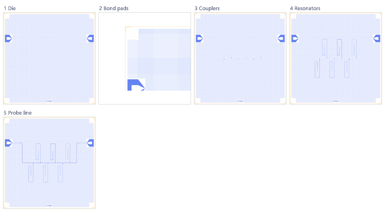
2 SMA8 launchers · 1 probe line · 6 spiral λ/4 resonators (5374 to 5589 µm) · 6 coupling capacitors |
Builds today |
yes (layout built on 2026-11-19 in 7 s) |
How it builds: Die, bond pads, couplers, resonators, probe line.
Numbers are from a run of this notebook on 2026-11-19 (Setup, Design, Check and the LOM cells, 16 s): QuCat normal modes with QuTiP dressed values.
mode |
kind |
f (GHz) |
κ (MHz) |
A (MHz) |
participation |
|---|---|---|---|---|---|
R5 |
resonator |
5.578 |
0.0652 |
0 |
R5 1.00 |
R0 |
resonator |
5.652 |
1.42 |
0 |
R0 1.00 |
R4 |
resonator |
5.682 |
0.0456 |
0 |
R4 1.00 |
R1 |
resonator |
5.688 |
0.739 |
0 |
R1 1.00 |
R3 |
resonator |
5.773 |
0.124 |
0 |
R3 1.00 |
R2 |
resonator |
5.795 |
0.226 |
0 |
R2 1.00 |
mode |
Q_ext (LOM) |
|---|---|
R0 |
3980 |
R1 |
7700 |
R2 |
25600 |
R3 |
46500 |
R4 |
125000 |
R5 |
85600 |
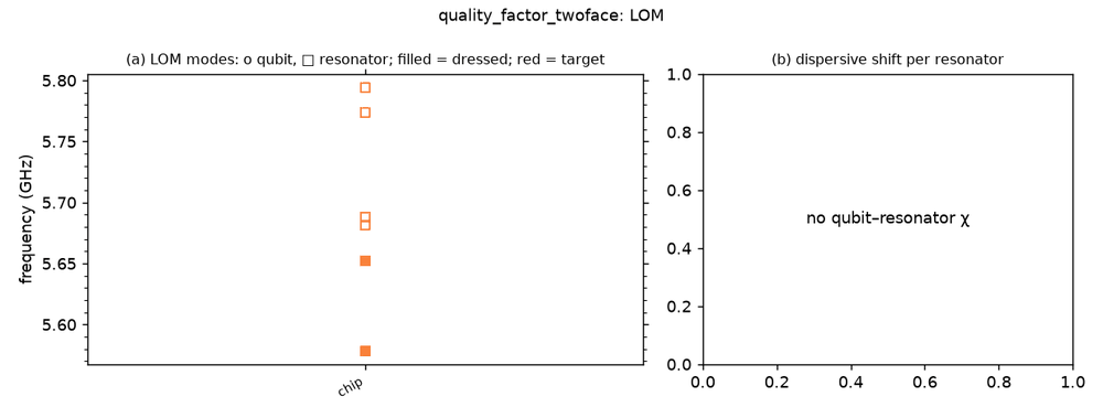
These are lumped-model estimates (component formulas and calibration), not FEM results; see the LOM page for how far to trust them.
sample_holder_test
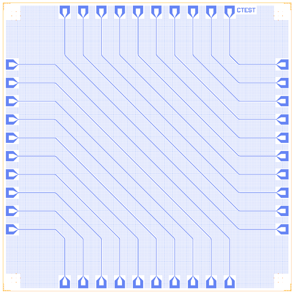
Tests: a 40-pad sample holder: every pad pair is joined by a line.
Notebook |
|
Source |
KQCircuits |
On the chip |
40 RF launchers (10 per side) · 20 CPWs |
Builds today |
yes (layout built on 2026-11-19 in 6 s) |
How it builds: Die, the 40 launchers, the 20 lines.
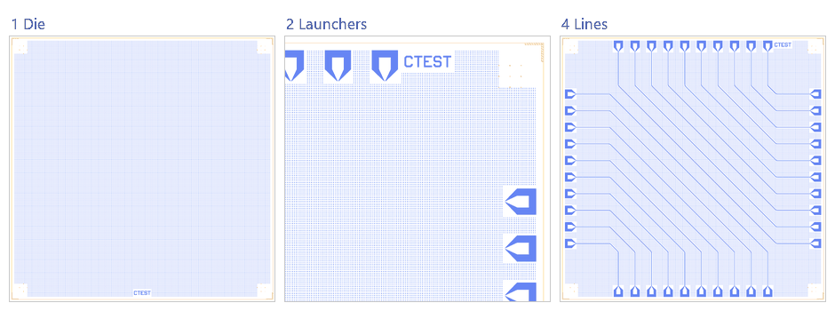
This chip has no junction or resonator (20 × 50 Ω through lines; the lengths are printed in Design 4), so there is no lumped-model estimate.
empty
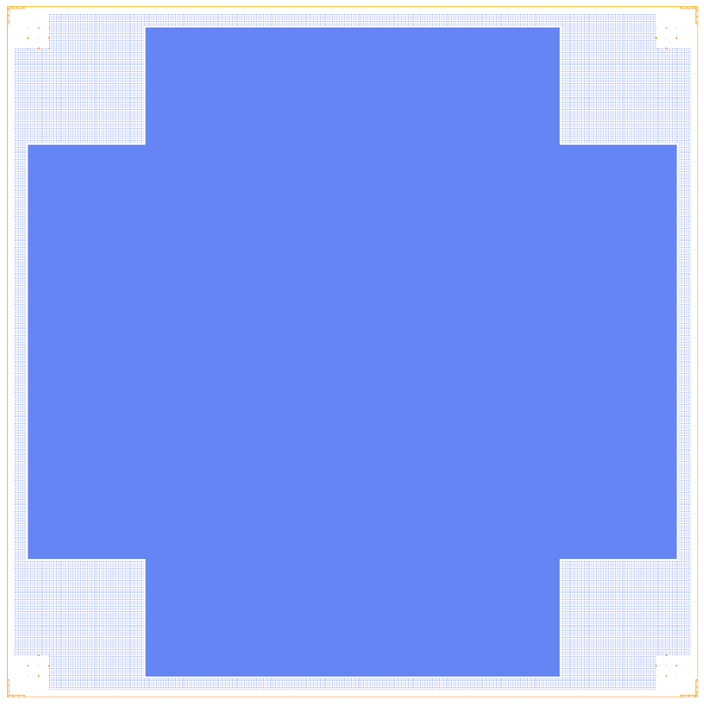
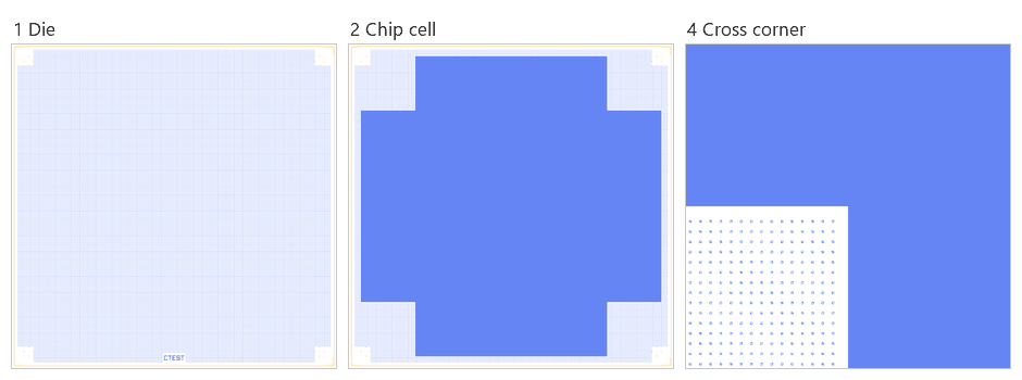
Tests: electron-beam lithography with the ground removed in a cross-shaped area.
Notebook |
|
Source |
KQCircuits |
On the chip |
one chip-level cross-shaped opening, no components |
Builds today |
yes (layout built on 2026-11-19 in 4 s) |
How it builds: Die, the chip cell, a view of the cross corner.
This chip has no junction, qubit or resonator, so there is no lumped-model estimate, and the notebook’s LOM section says there is nothing to simulate. The chip is measured in the process (optical or EBL inspection, DC probing) and not with microwaves.
junction_test
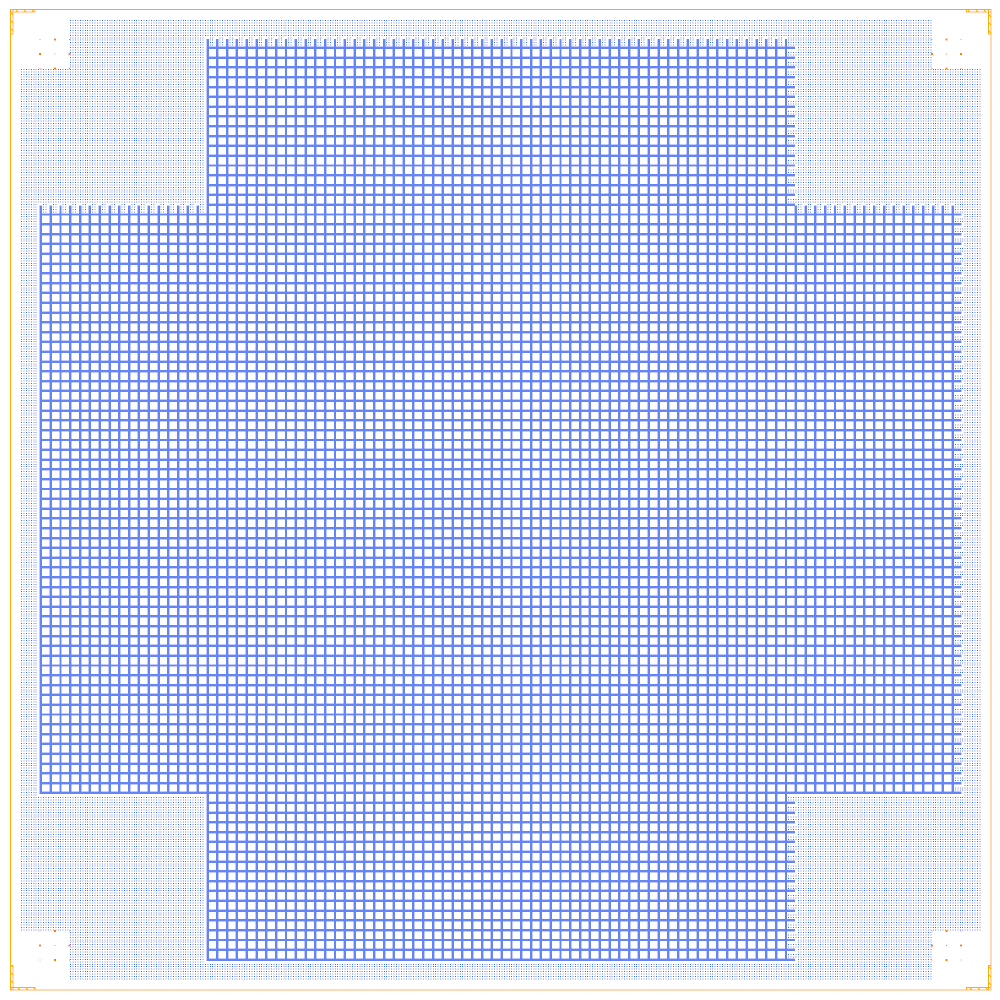
Tests: electron-beam lithography and junction process: a cross opening filled with an array of 80 × 80 µm squares.
Notebook |
|
Source |
KQCircuits |
On the chip |
one chip-level cross opening with a square array, no components |
Builds today |
yes (layout built on 2026-11-19 in 3 s) |
How it builds: Die, the chip cell, a view of the cross corner.
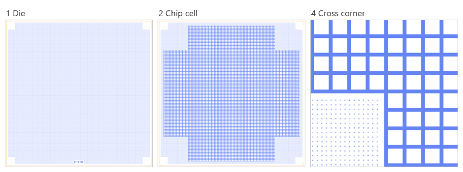
This chip has no junction, qubit or resonator, so there is no lumped-model estimate, and the notebook’s LOM section says there is nothing to simulate. The chip is measured in the process (optical or EBL inspection, DC probing) and not with microwaves.
junction_test2
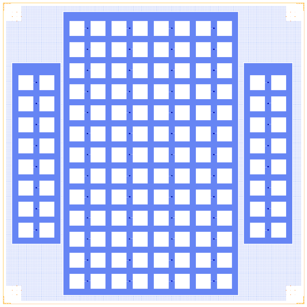
Tests: SQUID junction arrays on test pads, with stepped junction widths.
Notebook |
|
Source |
KQCircuits |
On the chip |
6 pad arrays, each with a Quantcore SQUID between its pad pairs |
Builds today |
yes (layout built on 2026-11-19 in 4 s) |
How it builds: Die, the chip cell, the pad arrays, one test SQUID.
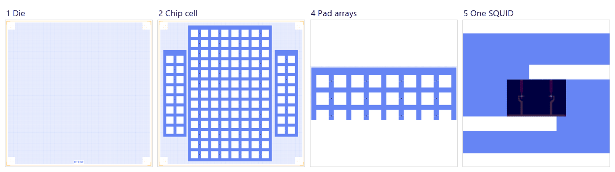
This chip has no modes to simulate, so there are no qubit or resonator estimates. Numbers are from a run of this notebook on 2026-11-19 (4 s): what the chip measures is each test SQUID’s R_n at room temperature, so the notebook lists the R_n and L_J the PDK junction rule gives each stepped finger (two junctions in parallel per SQUID; Nb Δ = 1.4 meV, R_n·A = 13.5 kΩ·µm² assumed).
array |
loop |
SQUIDs |
straight finger (µm) |
R_n per SQUID (kΩ) |
L_J per SQUID (nH) |
in 40-50 kΩ |
|---|---|---|---|---|---|---|
1 |
large (130 µm²) |
8 |
0.10 to 0.31 |
112.5 to 36.3 |
16.84 to 5.43 |
2 |
2 |
large (130 µm²) |
13 |
0.34 to 0.70 |
33.1 to 16.1 |
4.95 to 2.41 |
0 |
3 |
small (80 µm²) |
13 |
0.15 to 0.27 |
75.0 to 41.7 |
11.22 to 6.24 |
5 |
4 |
small (80 µm²) |
13 |
0.28 to 0.40 |
40.2 to 28.1 |
6.01 to 4.21 |
1 |
5 |
small (80 µm²) |
13 |
0.41 to 0.53 |
27.4 to 21.2 |
4.11 to 3.18 |
0 |
6 |
large (130 µm²) |
8 |
0.73 to 0.94 |
15.4 to 12.0 |
2.31 to 1.79 |
0 |
8 SQUIDs fall inside the PDK’s 40 to 50 kΩ window.
These are lumped-model estimates (component formulas and calibration), not FEM results; see the LOM page for how far to trust them.
lithography_test
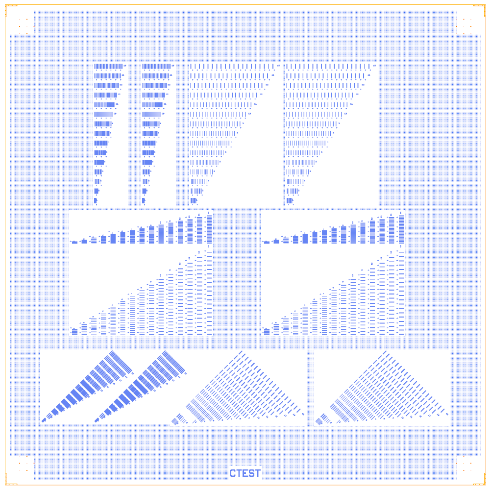
Tests: optical lithography resolution: stripe blocks with 1 to 15 µm lines, spaced 1 and 5 times the width, and crosses.
Notebook |
|
Source |
KQCircuits |
On the chip |
horizontal, vertical and diagonal line blocks, no components |
Builds today |
yes (layout built on 2026-11-19 in 3 s) |
How it builds: Die, the chip cell, horizontal, vertical and diagonal blocks.
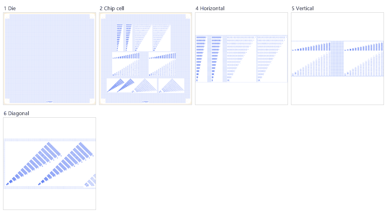
This chip has no junction, qubit or resonator, so there is no lumped-model estimate, and the notebook’s LOM section says there is nothing to simulate. The chip is measured in the process (optical or EBL inspection, DC probing) and not with microwaves.
lithography_test_twoface
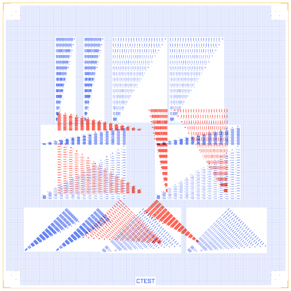
Tests: the same lithography test on both faces of a flip chip.
Notebook |
|
Source |
KQCircuits |
On the chip |
the line blocks of LithographyTest on the bottom chip, six mirrored blocks on the top chip |
Builds today |
yes (layout built on 2026-11-19 in 3 s) |
How it builds: Die, the chip cell, horizontal, vertical and diagonal blocks, top chip.
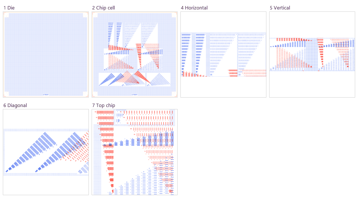
This chip has no junction, qubit or resonator, so there is no lumped-model estimate, and the notebook’s LOM section says there is nothing to simulate. The chip is measured in the process (optical or EBL inspection, DC probing) and not with microwaves.
stripes
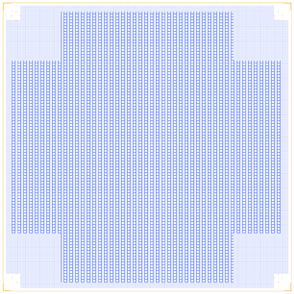
Tests: ground-grid and lithography stripes: 80 µm metal stripes at 200 µm pitch and 80 µm squares in a cross opening.
Notebook |
|
Source |
KQCircuits |
On the chip |
one chip-level cross opening with stripes, no components |
Builds today |
yes (layout built on 2026-11-19 in 3 s) |
How it builds: Die, the chip cell, a view of the cross corner.
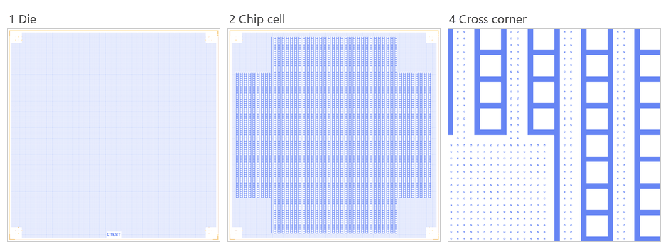
This chip has no junction, qubit or resonator, so there is no lumped-model estimate, and the notebook’s LOM section says there is nothing to simulate. The chip is measured in the process (optical or EBL inspection, DC probing) and not with microwaves.
tsv_test
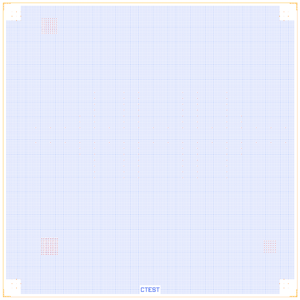
Tests: the through-silicon-via process: a TSV fence pattern and three metrology arrays for cross-sections.
Notebook |
|
Source |
KQCircuits |
On the chip |
1 |
Builds today |
yes (layout built on 2026-11-19 in 5 s) |
How it builds: Die, the chip cell, the centre pattern, a metrology array.
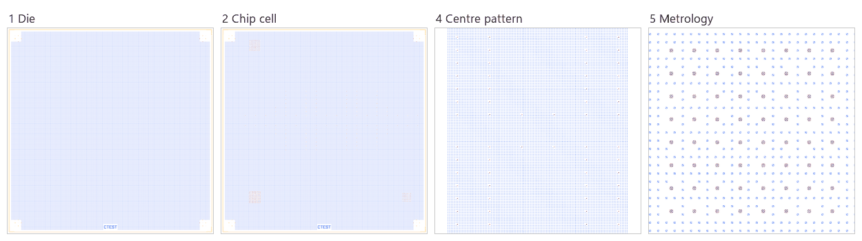
This chip has no junction, qubit or resonator, so there is no lumped-model estimate, and the notebook’s LOM section says there is nothing to simulate. The chip is measured in the process (optical or EBL inspection, DC probing) and not with microwaves.
Build spec
The rest of this page is the detailed spec the notebooks were built from: the sources, coordinates, routes and the build status of each chip.
Sources other-libs/KQCircuits-main/KQCircuits-main/klayout_package/python/kqcircuits/chips/<module>.py, GPL-3.0
(IQM Finland). Rebuilt from extracted parameters. All of them are 10 × 10 mm with box (0,0)–(10000,10000), and the
KQC frame = Designer frame. Coordinates come from a scratch build of each KQC chip on 2026-11-02. The “buildable now?” column below is per chip. launchers={"type": T, "assign": {pad: name}} reproduces
KQC launcher_assignments. Plain "SMA8" gives pads NW, NE, EN, ES, SE, SW, WS, WN at (2800,9200), (7200,9200),
(9200,7200), (9200,2800), (7200,800), (2800,800), (800,2800), (800,7200).
Components
chip (module) |
purpose |
main elements (catalog ref, params, placement) |
buildable now? |
|---|---|---|---|
JunctionTest ( |
EBL / junction process test |
One chip-level polygon in |
yes (placed as the whole KQC chip PCell, see the rebuild below) |
JunctionTest2 ( |
SQUID test-pad arrays |
6 × |
yes |
AirbridgeCrossings ( |
airbridge crossing + mechanical test |
SMA8 assign {1:PL-1-IN, 2:PL-2-IN, 3:PL-4-IN, 4:PL-4-OUT, 5:PL-2-OUT, 6:PL-1-OUT, 7:PL-3-OUT, 8:PL-3-IN}. Mechanical array: 19 lengths × 8 widths × 4 distances = 608 straight CPWs, |
built element by element ( |
AirbridgeDcTest ( |
4-point DC airbridge resistance |
22 × |
yes |
CrossingTwoface ( |
flip-chip crossing / crosstalk |
|
built element by element ( |
LithographyTest ( |
optical-litho resolution |
For each width w = 1…15 µm and spacing factor s ∈ {1, 5}: |
yes (script loops, ≈ 300 instances; KQC uses plain container cells) |
LithographyTestTwoface ( |
same, both faces |
The above on 1t1, plus 6 blocks on face 2b1 ( |
yes (compose transforms per item) |
TsvTest ( |
through-silicon-via process |
|
yes |
Stripes ( |
ground-grid / litho stripes |
Chip-level polygon (cross opening 2000–8000) minus 80 µm-wide stripes at 200 µm pitch and 80 µm squares ( |
yes (placed as the whole KQC chip PCell, see the rebuild below) |
Shaping ( |
readout with Purcell filter (1 qubit) |
|
built element by element ( |
DcTest ( |
DC sample-holder pads |
|
yes |
Empty ( |
EBL test, ground removed |
Chip-level polygon in |
yes (placed as the whole KQC chip PCell, see the rebuild below) |
Launchers ( |
bare sample-holder pads |
|
yes |
Simple ( |
minimal connected chip |
SMA8 |
yes (verified: 6 route lengths = KQC, LOM fully connected) |
SampleHolderTest ( |
40-pad holder test |
40 RF pads (width 160, gap 96, indent 520, pitch 635), 10 per side, paired by 20 CPWs. Designer |
built element by element ( |
QualityFactorTwoface ( |
flip-chip (capped) spiral λ/4 Q test |
|
built element by element ( |
Routes
AirbridgeCrossings: PL-1 chip.PL-1-IN → chip.PL-1-OUT, straight x = 2800. PL-2 is straight at x = 7200. PL-3 runs chip.PL-3-IN (800,7200) → chip.PL-3-OUT (800,2800) and weaves across x = 2800 20 times, with step = 4400 / 9.5 / 2 = 231.58 and wiggle 250. Per pair: (2550,y), wp((2800,y), airbridge=True), (3050,y); y −= step; (3050,y), wp((2800,y), airbridge=True), (2550,y); y −= step. PL-4 runs EN → ES weaving between x = 7500 and 8000 (no crossing).
CrossingTwoface (a_capped = b_capped = 10 on the top-chip span): PL-1 NW → SW: (2800,8900), (4300,8900), wp((4300,8500), a=10, b=10), wp((4300,1600), a=10, b=6), (4300,1100), (2800,1100). PL-2 likewise at x = 5700 from NE → SE. PL-3 runs WN → WS: wp((1500,7200), a=10, b=10), then 3 × [(3850,y), wp((4100,y), face_id=”2b1”), wp((4500,y), face_id=”1t1”), (4750,y); y −= 880; mirrored back], then wp((1600,2800), a=10, b=6), (900,2800). This crosses PL-1 on the top chip. PL-4 runs EN → ES: (9100,7200), wp((8500,7200), a=10, b=10), 3 × wiggle 6000 ↔ 6900 (step 880), wp((8400,2800), a=10, b=6), (9100,2800).
Simple: WN → Swissmon.flux; Swissmon.cplr1 → C1.a; C1.b → T.left; T.right → EN; T.bottom → C2.a; C2.b → SE. All are straight cpw.
Shaping: chargeline WN → drive via (900,7200), (900,5150), (3750,5150),
term2=6. Fluxline WS → flux via (900,2800), (900,5000), (3687.67,5000). Per chain: qubit → T_a (meander 1681.76 to T_b) → T_b stub shorted (580.6) → J cap → T_c (stub shorted 758.6) → Purcell meander 2479.24 → κ cap → output to EN (top) / ES (bottom). The drive cap goes from T_a.bottom to NW / SW.SampleHolderTest: PL-i (i = 1…10) N pad (x_i = 2142.5+635(i−1)) → (x_i, 8180) → (8180, y_i = x_i) → E pad. PL-(11+k) (k = 0…9) S pad (x = 7857.5−635k) → (x, 1820) → (1820, 7857.5−635k) → W pad. The middle segments are diagonal and nested.
QualityFactorTwoface: probe line PL-1-IN (800,7200) → taper to a/b = 10/10 at (1500,7200) → (2000,7200) → (2000,5000) → T0 … T5 → (8000,5000) → (8000,7200) → taper back to 10/6 at (8400,7200) → PL-1-OUT. KQC’s face nodes at (2300,5000) and (7700,5000) go to face 0, i.e. no face change with the defaults. Each spiral: capacitor port b → KQC’s polygon spiral (one and a half turns in the 2000 × 500 box) → shorted end (term 0).
AirbridgeDcTest, JunctionTest2, TsvTest, LithographyTest*, DcTest, Launchers: no routes.
Launchers, pads, test structures, markers, labels
Covered per chip above. Every chip gets the KQC chip frame and markers from the DesignChip base. DcTest/Launchers are the pads themselves.
LOM node structure (qubit ↔ resonator ↔ feedline ↔ bus ↔ control lines)
Only Shaping and Simple have a qubit. In Simple, the Swissmon flux port takes the WN line (a control), and cplr1
feeds C1 → T → EN with C2 to SE. Shaping’s resonators are tapped (T’s inside the λ/4). As built, every
piece of a chain is a cpw route (the meanders too, on KQC’s Meander centre line), so the LOM builder makes each chain
one λ/4 TLres of the summed route length (the T arms, 306 / 153 µm, are not counted) with the drive and J capacitors
on its coupler-end node: right mode structure (qubit, 2 readouts, 2 Purcell filters), rough couplings. A Meander
instance or a meander route between two T’s would instead become a λ/2 bus (wrong). QualityFactorTwoface: six λ/4
spiral routes behind finger/gap capacitors on one probe-line conductor between two 50 Ω launchers. The other chips
have no circuit LOM: transmission lines only, or DC/process structures (AirbridgeCrossings’ 1280 mechanical-test
bridges are ground straps; the LOM Airbridge model is a wire, so their unconnected ports have no node yet).
Targets (if stated)
Shaping: segment_length_target_rr=[611.586, 1834.76, 611.586], segment_length_target_pr=[3158.32, 789.581],
caps_length=[37.5, 67.9, 36.2] (J, κ, drive). The others give no targets.
Simplifications for a first rebuild
Build Simple first: it is the smoke test for KQC parity. AirbridgeDcTest, JunctionTest2, TsvTest and DcTest are pure placement. The polygon-only chips (JunctionTest, Stripes, Empty) are placed as the whole KQC chip PCell.
Quantcore PDK rebuild
Each notebook is a Quantcore-PDK rebuild of the source chip. The netlist, LOM and imported components are kept, and the process is Quantcore’s.
Chip: the Quantcore die frame (L dicing markers 1000/0, 3 × 3 alignment grids 1001/0, chip boundary 100/0, device ID where an edge is free; any brand text is QCT), drawn on the source’s 10 × 10 mm chip (its launchers sit on the chip edges, so the design does not fit the 7.5 mm die). KQC’s ChipFrame (dicing edge, corner markers, labels) is not drawn. KQC’s original grids its whole ground plane (
with_grid, 5 µm squares on a 10 µm step). The rebuild keeps that coverage at the PDK density instead (chip parametercheese: "chip",with_grid: false): 5 µm squares with 20 µm gaps over the whole die, at least 4 µm from the 3/0 keep-outs, inside the design area and clear of the frame markers and the device ID.Stack: sapphire 650 µm, εr 10.25 (the PDK default stack, used by the LOM estimates and every FEM export); KQC’s own simulation default is silicon (εr 11.45), so LOM capacitances and resonator frequencies here are for sapphire.
Junctions: Quantcore Nb/AlOx/Nb trilayer junctions (
junction_typefromlayouts.registry.trilayer_junction): fingers on 2/0 + 4/0, spacer 50/0 with the 51–53/0 gradient, sized on the PDK junction rule (Nb Δ = 1.4 meV, I_c·R_n = πΔ/2e, R_n·A 13.5 kΩ·µm² and C_J 50 fF/µm² assumed); the Swissmon’s SQUID becomes a PDK SQUID of two 0.25 × 0.6 µm junctions → R_n = 45 kΩ in parallel, L_J = 6.73 nH at zero flux, C_J = 15 fF (in the 40–50 kΩ window). KQC’sjunction_widthsets the straight finger. This replaces the assumed Lj 12 nH + 2 fF. Expected f_q ≈ 6.0 GHz (was 4.74 GHz; estimate from the pre-rebuild LOM C_Σ).Kept: the topology and every KQC element with the source’s parameters, positions and orientations, the launcher assignment, every route’s path and length, the sim groups.
Chip: the Quantcore die frame (L dicing markers 1000/0, 3 × 3 alignment grids 1001/0, chip boundary 100/0, device ID where an edge is free; any brand text is QCT), drawn on the source’s 10 × 10 mm chip (its launchers sit on the chip edges, so the design does not fit the 7.5 mm die). KQC’s ChipFrame (dicing edge, corner markers, labels) is not drawn. KQC’s original grids its whole ground plane (
with_grid, 5 µm squares on a 10 µm step). The rebuild keeps that coverage at the PDK density instead (chip parametercheese: "chip",with_grid: false): 5 µm squares with 20 µm gaps over the whole die, at least 4 µm from the 3/0 keep-outs, inside the design area and clear of the frame markers and the device ID.Stack: sapphire 650 µm, εr 10.25 (the PDK default stack, used by the LOM estimates and every FEM export); KQC’s own simulation default is silicon (εr 11.45), so LOM capacitances and resonator frequencies here are for sapphire.
Junctions: Quantcore Nb/AlOx/Nb trilayer junctions (
junction_typefromlayouts.registry.trilayer_junction): fingers on 2/0 + 4/0, spacer 50/0 with the 51–53/0 gradient, sized on the PDK junction rule (Nb Δ = 1.4 meV, I_c·R_n = πΔ/2e, R_n·A 13.5 kΩ·µm² and C_J 50 fF/µm² assumed); the Swissmon’s SQUID becomes a PDK SQUID of two 0.25 × 0.6 µm junctions → R_n = 45 kΩ in parallel, L_J = 6.73 nH at zero flux, C_J = 15 fF (in the 40–50 kΩ window). KQC’sjunction_widthsets the straight finger. This replaces the assumed Lj 12 nH + 2 fF. Expected f_q ≈ 6.4 GHz (was 5.17 GHz), below the ≈ 8.5 GHz readout (estimate from the pre-rebuild LOM C_Σ).Kept: the topology and every KQC element with the source’s parameters, positions and orientations, the launcher assignment, every route’s path and length, the sim groups (KQC’s
cap_paramscapacitors, every straight with KQC’s length formula).
Chip: the Quantcore die frame (L dicing markers 1000/0, 3 × 3 alignment grids 1001/0, chip boundary 100/0, device ID where an edge is free; any brand text is QCT), drawn on the source’s 10 × 10 mm chip (its launchers sit on the chip edges, so the design does not fit the 7.5 mm die). KQC’s ChipFrame (dicing edge, corner markers, labels) is not drawn. KQC’s original grids its whole ground plane (
with_grid, 5 µm squares on a 10 µm step). The rebuild keeps that coverage at the PDK density instead (chip parametercheese: "chip",with_grid: false): 5 µm squares with 20 µm gaps over the whole die, at least 4 µm from the 3/0 keep-outs, inside the design area and clear of the frame markers and the device ID.Stack: sapphire 650 µm, εr 10.25 (the PDK default stack, used by the LOM estimates and every FEM export); KQC’s own simulation default is silicon (εr 11.45), so LOM capacitances and resonator frequencies here are for sapphire.
Junctions: none on this chip (no qubits or junctions).
Kept: the topology and every KQC element with the source’s parameters, positions and orientations, the launcher assignment, every route’s path and length, the sim groups (the 20 crossings, the 608-CPW / 1280-bridge array; airbridges on 300/0 + 301/0).
Chip: the Quantcore die frame (L dicing markers 1000/0, 3 × 3 alignment grids 1001/0, chip boundary 100/0, device ID where an edge is free; any brand text is QCT), drawn on the source’s 10 × 10 mm chip (its launchers sit on the chip edges, so the design does not fit the 7.5 mm die). KQC’s ChipFrame (dicing edge, corner markers, labels) is not drawn. KQC’s original grids its whole ground plane (
with_grid, 5 µm squares on a 10 µm step). The rebuild keeps that coverage at the PDK density instead (chip parametercheese: "chip",with_grid: false): 5 µm squares with 20 µm gaps over the whole die, at least 4 µm from the 3/0 keep-outs, inside the design area and clear of the frame markers and the device ID. The top chip (face 2b1) gets no frame, because PDK v3 defines none for the flip-chip top chip (its layers export to 800–804/0).Stack: sapphire 650 µm, εr 10.25 (the PDK default stack, used by the LOM estimates and every FEM export); KQC’s own simulation default is silicon (εr 11.45), so LOM capacitances and resonator frequencies here are for sapphire.
Junctions: none on this chip (no qubits or junctions).
Kept: the topology and every KQC element with the source’s parameters, positions and orientations, the launcher assignment, every route’s path and length, the sim groups (both faces, the face changes and flip-chip connectors).
Chip: the Quantcore die frame (L dicing markers 1000/0, 3 × 3 alignment grids 1001/0, chip boundary 100/0, device ID where an edge is free; any brand text is QCT), drawn on the source’s 10 × 10 mm chip (its launchers sit on the chip edges, so the design does not fit the 7.5 mm die). KQC’s ChipFrame (dicing edge, corner markers, labels) is not drawn. KQC’s original grids its whole ground plane (
with_grid, 5 µm squares on a 10 µm step). The rebuild keeps that coverage at the PDK density instead (chip parametercheese: "chip",with_grid: false): 5 µm squares with 20 µm gaps over the whole die, at least 4 µm from the 3/0 keep-outs, inside the design area and clear of the frame markers and the device ID. The top chip (face 2b1) gets no frame, because PDK v3 defines none for the flip-chip top chip (its layers export to 800–804/0).Stack: sapphire 650 µm, εr 10.25 (the PDK default stack, used by the LOM estimates and every FEM export); KQC’s own simulation default is silicon (εr 11.45), so LOM capacitances and resonator frequencies here are for sapphire.
Junctions: none on this chip (no qubits or junctions).
Kept: the topology and every KQC element with the source’s parameters, positions and orientations, the launcher assignment, every route’s path and length, the sim groups (resonator lengths 5374–5589 µm, the capped-CPW probe line, the top-chip lid).
Chip: the Quantcore die frame (L dicing markers 1000/0, 3 × 3 alignment grids 1001/0, chip boundary 100/0, device ID where an edge is free; any brand text is QCT), drawn on the source’s 10 × 10 mm chip (its launchers sit on the chip edges, so the design does not fit the 7.5 mm die). KQC’s ChipFrame (dicing edge, corner markers, labels) is not drawn. KQC’s original grids its whole ground plane (
with_grid, 5 µm squares on a 10 µm step). The rebuild keeps that coverage at the PDK density instead (chip parametercheese: "chip",with_grid: false): 5 µm squares with 20 µm gaps over the whole die, at least 4 µm from the 3/0 keep-outs, inside the design area and clear of the frame markers and the device ID.Stack: sapphire 650 µm, εr 10.25 (the PDK default stack, used by the LOM estimates and every FEM export); KQC’s own simulation default is silicon (εr 11.45), so LOM capacitances and resonator frequencies here are for sapphire.
Junctions: none on this chip (no qubits or junctions).
Kept: the topology and every KQC element with the source’s parameters, positions and orientations, the launcher assignment, every route’s path and length, the sim groups (KQC’s
produce_n_launchers(40, …)and the 20 lines).
Chip: the Quantcore die frame (L dicing markers 1000/0, 3 × 3 alignment grids 1001/0, chip boundary 100/0, device ID where an edge is free; any brand text is QCT), drawn on the source’s 10 × 10 mm chip. The KQC chip PCell is placed with
frames_enabled=[], so its own ChipFrame (dicing edge, markers, labels) is not drawn. KQC’s original grids its whole ground plane (with_grid, 5 µm squares on a 10 µm step). The rebuild keeps that coverage at the PDK density instead (chip parametercheese: "chip",with_grid: false): 5 µm squares with 20 µm gaps over the whole die, at least 4 µm from the 3/0 keep-outs, inside the design area and clear of the frame markers and the device ID.Stack: sapphire 650 µm, εr 10.25 (the PDK default stack, used by the LOM estimates and every FEM export); KQC’s own simulation default is silicon (εr 11.45), so LOM capacitances and resonator frequencies here are for sapphire.
Junctions: none on this chip (no qubits or junctions).
Kept: the whole KQC chip PCell with the source’s parameters (KQC’s own
build()).
Chip: the Quantcore die frame (L dicing markers 1000/0, 3 × 3 alignment grids 1001/0, chip boundary 100/0, device ID where an edge is free; any brand text is QCT), drawn on the source’s 10 × 10 mm chip. The KQC chip PCell is placed with
frames_enabled=[], so its own ChipFrame (dicing edge, markers, labels) is not drawn. KQC’s original grids its whole ground plane (with_grid, 5 µm squares on a 10 µm step). The rebuild keeps that coverage at the PDK density instead (chip parametercheese: "chip",with_grid: false): 5 µm squares with 20 µm gaps over the whole die, at least 4 µm from the 3/0 keep-outs, inside the design area and clear of the frame markers and the device ID: here the four ground corners outside the cross opening and the band along the die edge (the opening itself has no metal).Stack: sapphire 650 µm, εr 10.25 (the PDK default stack, used by the LOM estimates and every FEM export); KQC’s own simulation default is silicon (εr 11.45), so LOM capacitances and resonator frequencies here are for sapphire.
Junctions: none on this chip (no qubits or junctions).
Kept: the whole KQC chip PCell with the source’s parameters (KQC’s own
build()).
Chip: the Quantcore die frame (L dicing markers 1000/0, 3 × 3 alignment grids 1001/0, chip boundary 100/0, device ID where an edge is free; any brand text is QCT), drawn on the source’s 10 × 10 mm chip. The KQC chip PCell is placed with
frames_enabled=[], so its own ChipFrame (dicing edge, markers, labels) is not drawn. The PDK cheese (5 µm squares with 20 µm gaps, at least 4 µm from the 3/0 keep-outs) covers the whole die (chip parametercheese: "chip"): the ground round the cross, its corners included; the 80 µm squares inside the cross stay solid.Stack: sapphire 650 µm, εr 10.25 (the PDK default stack, used by the LOM estimates and every FEM export); KQC’s own simulation default is silicon (εr 11.45), so LOM capacitances and resonator frequencies here are for sapphire.
Junctions: none on this chip (the KQC cell draws EBL test squares, no junctions).
Kept: the whole KQC chip PCell with the source’s parameters (KQC’s own
build()).
Chip: the Quantcore die frame (L dicing markers 1000/0, 3 × 3 alignment grids 1001/0, chip boundary 100/0, device ID where an edge is free; any brand text is QCT), drawn on the source’s 10 × 10 mm chip. The KQC chip PCell is placed with
frames_enabled=[], so its own ChipFrame (dicing edge, markers, labels) is not drawn. The PDK cheese (5 µm squares with 20 µm gaps, at least 4 µm from the 3/0 keep-outs) covers the whole die (chip parametercheese: "chip").Stack: sapphire 650 µm, εr 10.25 (the PDK default stack, used by the LOM estimates and every FEM export); KQC’s own simulation default is silicon (εr 11.45), so LOM capacitances and resonator frequencies here are for sapphire.
Junctions: none on this chip (no qubits or junctions).
Kept: the whole KQC chip PCell with the source’s parameters (KQC’s own
build()).
Chip: the Quantcore die frame (L dicing markers 1000/0, 3 × 3 alignment grids 1001/0, chip boundary 100/0, device ID where an edge is free; any brand text is QCT), drawn on the source’s 10 × 10 mm chip. The KQC chip PCell is placed with
frames_enabled=[], so its own ChipFrame (dicing edge, markers, labels) is not drawn. The PDK cheese (5 µm squares with 20 µm gaps, at least 4 µm from the 3/0 keep-outs) covers the whole die (chip parametercheese: "chip"). The top chip (face 2b1) gets no frame, because PDK v3 defines none for the flip-chip top chip (its layers export to 800–804/0).Stack: sapphire 650 µm, εr 10.25 (the PDK default stack, used by the LOM estimates and every FEM export); KQC’s own simulation default is silicon (εr 11.45), so LOM capacitances and resonator frequencies here are for sapphire.
Junctions: none on this chip (no qubits or junctions).
Kept: the whole KQC chip PCell with the source’s parameters (KQC’s own
build()).
Chip: the Quantcore die frame (L dicing markers 1000/0, 3 × 3 alignment grids 1001/0, chip boundary 100/0, device ID where an edge is free; any brand text is QCT), drawn on the source’s 10 × 10 mm chip. The KQC chip PCell is placed with
frames_enabled=[], so its own ChipFrame (dicing edge, markers, labels) is not drawn. The PDK cheese (5 µm squares with 20 µm gaps, at least 4 µm from the 3/0 keep-outs) covers the whole die (chip parametercheese: "chip"): the ground round the cross, its corners included, and a row of holes down the middle of each wider metal stripe inside the cross.Stack: sapphire 650 µm, εr 10.25 (the PDK default stack, used by the LOM estimates and every FEM export); KQC’s own simulation default is silicon (εr 11.45), so LOM capacitances and resonator frequencies here are for sapphire.
Junctions: none on this chip (no qubits or junctions).
Kept: the whole KQC chip PCell with the source’s parameters (KQC’s own
build()).
Chip: the Quantcore die frame (L dicing markers 1000/0, 3 × 3 alignment grids 1001/0, chip boundary 100/0, device ID where an edge is free; any brand text is QCT), drawn on the source’s 10 × 10 mm chip. The KQC chip PCell is placed with
frames_enabled=[], so its own ChipFrame (dicing edge, markers, labels) is not drawn. KQC’s original grids its whole ground plane (with_grid, 5 µm squares on a 10 µm step). The rebuild keeps that coverage at the PDK density instead (chip parametercheese: "chip",with_grid: false): 5 µm squares with 20 µm gaps over the whole die, at least 4 µm from the 3/0 keep-outs, inside the design area and clear of the frame markers and the device ID. The top chip (face 2b1) gets no frame, because PDK v3 defines none for the flip-chip top chip (its layers export to 800–804/0).Stack: sapphire 650 µm, εr 10.25 (the PDK default stack, used by the LOM estimates and every FEM export); KQC’s own simulation default is silicon (εr 11.45), so LOM capacitances and resonator frequencies here are for sapphire.
Junctions: none on this chip (no qubits or junctions).
Kept: the whole KQC chip PCell with the source’s parameters (KQC’s own
build()).
Chip: the Quantcore die frame (L dicing markers 1000/0, 3 × 3 alignment grids 1001/0, chip boundary 100/0, device ID where an edge is free; any brand text is QCT), drawn on the source’s 10 × 10 mm chip. The KQC chip PCell is placed with
frames_enabled=[], so its own ChipFrame (dicing edge, markers, labels) is not drawn. KQC’s original grids its whole ground plane (with_grid, 5 µm squares on a 10 µm step). The rebuild keeps that coverage at the PDK density instead (chip parametercheese: "chip",with_grid: false): 5 µm squares with 20 µm gaps over the whole die, at least 4 µm from the 3/0 keep-outs, inside the design area and clear of the frame markers and the device ID.Stack: sapphire 650 µm, εr 10.25 (the PDK default stack, used by the LOM estimates and every FEM export); KQC’s own simulation default is silicon (εr 11.45), so LOM capacitances and resonator frequencies here are for sapphire.
Junctions: Quantcore Nb/AlOx/Nb trilayer junctions (
junction_typefromlayouts.registry.trilayer_junction): fingers on 2/0 + 4/0, spacer 50/0 with the 51–53/0 gradient, sized on the PDK junction rule (Nb Δ = 1.4 meV, I_c·R_n = πΔ/2e, R_n·A 13.5 kΩ·µm² and C_J 50 fF/µm² assumed); every test SQUID is a Quantcore SQUID (junction_type="Quantcore Squid"on the chip cell): KQC’s steppedjunction_widthis the straight finger, the bent finger stays 0.6 µm. KQC’s large-loop sweep starts at 0.08 µm, below the PDK minimum finger (0.1 µm), so it starts at 0.10 µm here (step 0.03 µm kept); the small-loop sweep keeps 0.15 µm + 0.01 µm steps. Per SQUID, R_n then spans ≈ 75 → 21 kΩ (small loops, 0.15–0.53 µm) and ≈ 113 → 12 kΩ (large loops, 0.10–0.94 µm), across the 40–50 kΩ window (section 4).Kept: the whole KQC chip PCell with the source’s parameters (KQC’s own
build()) (the six arrays, pad sizes, loop areas, the step sizes).