Write your own notebook
This page shows how to turn your own chip into a notebook that runs the whole design loop. You start from a template that already builds a tiny chip (one Xmon and one λ/4 readout) and runs as far as the LOM without a solver, then change it one segment at a time. Use it when none of the tutorials or design notebooks is close enough to your chip.
The loop the template follows:
layout → LOM → eigenmode simulations of the components → the same mesh for the FEM runs → extract and analyse → feedback
Copy and rename
Copy
examples/templates/full_loop_template.ipynbinto your own folder, for exampleexamples/mine/.Rename it. In section 0 set
NAME(the chip and its design file),OUT(where its JSON and pictures go) and the die size.Open it in Jupyter, with KLayout running to watch every change, or run headless with
QCC_LIVE=0.
Every cell you are expected to change is marked # TODO:. The notebook is split with # headings that match the
sections below.
Set the switches and the targets
The switch cell in section 0 decides what may run.
Switch |
Meaning |
|---|---|
|
no AEDT is started; FEM cells export jobs and load kept results |
|
fast solver settings (minutes, not converged) |
|
|
|
revisions the iterate cell may try |
|
your targets, in GHz |
Leave RUN_FEM = False on a small PC. Set it to True only on the simulation PC.
Change the layout, one segment at a time
Section 1 builds the chip in seven segments. After each one layout_step draws a picture and prints what the chip holds
so far, so you see what the change did.

Segments 1 to 5 of the template chip: the die, a bond pad, the feedline, the Xmon, the readout resonator.
Segment |
What you change |
|---|---|
1.1 Die |
the die size and chip ID |
1.2 Pads |
where the pads sit on the feedline height; |
1.3 Feedline |
the route between the pads |
1.4 Qubit |
the qubit class and its dimensions; the junction is sized from your target |
1.5 Readout |
the coupling length and where the hanger meets the feedline |
1.6 Control lines |
empty in the template; add your drive or flux line here |
1.7 Whole chip |
targets, the sim group, centring, |
Segment 1.7 writes <NAME>.json. That file is the deliverable: qcc build, qcc mask, the KLayout plugin and the
dashboard read it. The next cell runs the DRC; fix errors before going on (margins are warnings).
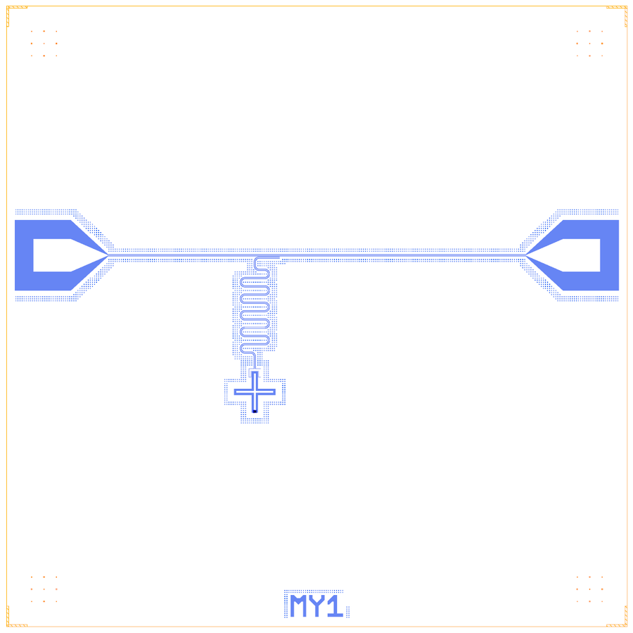
The whole template chip after segment 1.7.
Run the LOM
Section 2 turns the layout into a lumped circuit and solves it in seconds. This is where you iterate.
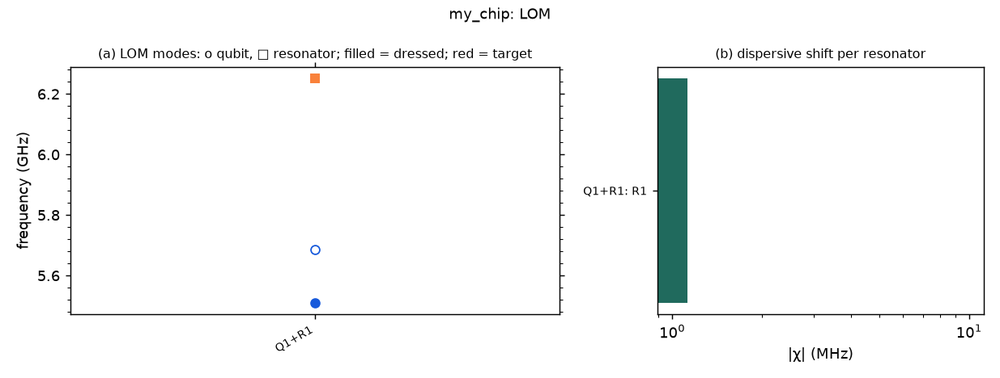
The LOM of the first build: the qubit is close to 5.5 GHz, the readout (squares) lands low, near 6.25 GHz.
The table puts each value next to its target. On the shipped chip the qubit is at 5.51 GHz (target 5.5) and the readout at 6.25 GHz (target 7.0): the claw loads the quarter-wave line. The next cell scales the readout length (λ/4 ∝ 1/f) until the LOM reads 6.99 GHz, then saves the design again. The save reports “The design differs”: that is the tuned length. These numbers are lumped-model estimates; the LOM page says how far to trust them.
Decide what to simulate
Sections 3 and 4 are the FEM part. They always export the jobs; they solve only with RUN_FEM = True.
Section |
Job |
Needs the simulation PC |
Why |
|---|---|---|---|
3 Eigenmode |
the sim group’s eigenmode job |
yes, to solve |
the modes, their Q and the junction participation |
4.1 Q3D |
the same group’s capacitance matrix |
yes, to solve |
measured capacitances for the LOM |
4.2 Driven |
|
yes, to solve |
the readout notch and κ |
The sim group is declared in segment 1.7 (d.sim_subset(...)): the part of the chip that a job cuts out. Keep it small:
a qubit with its readout, not the whole chip. Each of these sections starts with the marker “Simulation PC (32 GB+ RAM)”. The
library cannot reuse a solved mesh in a driven setup, so driven_from_eigenmode copies the eigenmode job’s mesh seeds and
frequency instead.
Read the results
Section 5 brings the FEM numbers into the LOM’s terms.
fillreplaces the LOM’s capacitance estimates with the Q3D values.epr_valuesanddriven_valuesread f_q, α, χ, f_r and κ from the eigenmode and driven jobs.The FEM against LOM table gives each quantity with the difference in %.
The plot and EPR cells (
plot_convergence,plot_s21_fit,plot_epr, the lumped EPR) print “not available yet” when their helper is missing, or show the plot.
Without results every cell prints one line saying what would appear. Put kept results in <OUT>/fem/<job>/ (copy the
folder from the simulation PC) and the same cells fill in on any PC.
Run the feedback
Section 6 is the loop.
target_copywrites your targets into a copy of the design, so the design file keeps its own.loop.analyseruns every estimator and picks one value per quantity (the consensus), with its residual in tolerances. Kept Q3D results are passed in asFILL.loop.feedbackproposes new knob values (junction L_J, readout length, claw) and writes revision 1, built and checked.iterate_to_targetrepeats until every target is inside its tolerance orMAX_ITERrevisions were made.
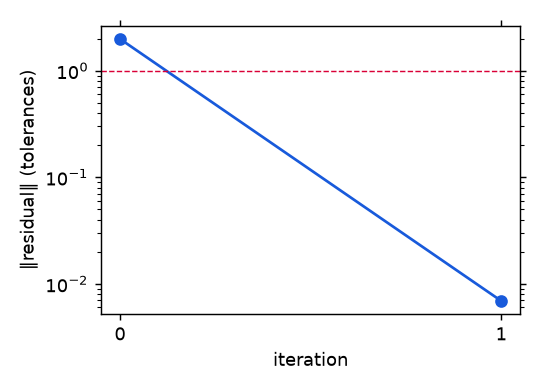
The residual falls below one tolerance in one revision (on the LOM).
A revision is only a file. To adopt it, set ADOPT = True in 6.3 (it copies the revision over your design file), then
carry the new numbers into your cells. Section 7 exports the mask.
Habits that keep it working
save_designat the end of the layout. It tells you whether the file changed. Do not hand-edit the JSON.One change at a time. Change one segment, run from there down, read the picture and the DRC, then go on.
Keep FEM results in
fem/.build/can be wiped;<OUT>/fem/is where kept results live and where the cells look.Targets in a copy.
target_copykeeps the deliverable clean.Do not solve twice.
RESOLVE = Falseloads kept results when they match the design.Margins are warnings. Errors must be zero; pad edge, keep-outs and centring are reported, not blocking.
Where to look next
The designer API and the component libraries for what you can place.
The LOM, simulation and feedback pages for what each section calls.
Lumped EPR for the participation helpers.
How a design notebook works: the longer form with eight design segments.