DemoQPU17 surface-17
A 17-qubit surface-code demo: 17 star transmons on a 5 × 5 grid (9 data, 8 auxiliary), 24 fixed couplers, a hairpin readout with its own Purcell filter per qubit on four feedlines, and an XY and a Z line per qubit. It is DeviceLayout.jl’s DemoQPU17 example (AWS, MIT), shaped after the ETH Zurich surface-17 device, rebuilt on the Quantcore PDK (GPL-3.0).
This is a plan-driven chip: the shared surface-17 generator first plans every instance and line, then the notebook places them kind by kind. It is a large build (117 instances, 154 routes).
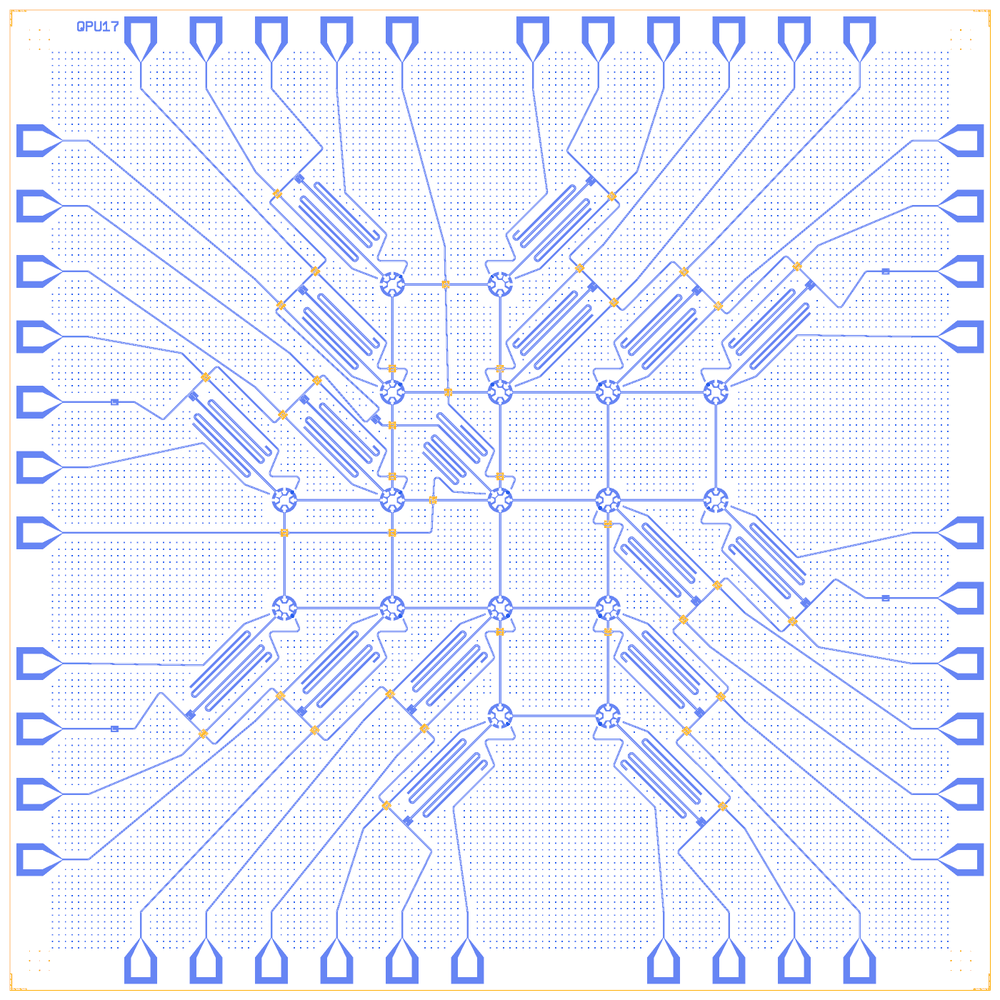
At a glance
Notebook |
|
Source |
DeviceLayout.jl |
Chip |
15 × 15 mm Quantcore die, sapphire 650 µm |
On the chip |
17 |
Builds today |
yes (layout built on 2026-11-19 in 31 s) |
How the notebook builds it
Each Design segment is one cell with one picture of the chip so far (see the notebook template).
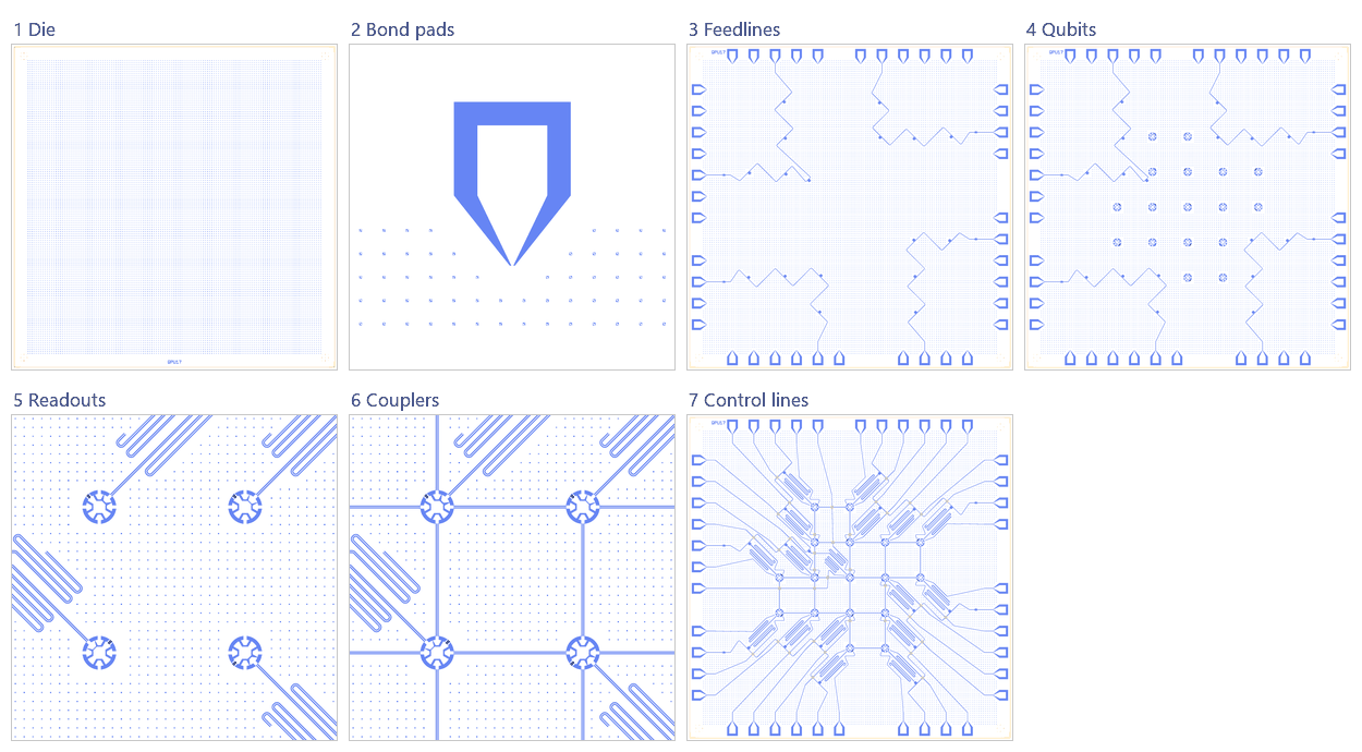
Die. The 15 × 15 mm die with the QCT frame, the lattice centre at the die centre.
Bond pads. The generator’s pads, moved to the 100 µm pad-edge rule.
Feedlines. The capacitive tees, the input capacitors and the four feedlines.
Qubits. The 17 star transmons, with junctions sized per qubit.
Readouts. The readout and Purcell λ/4 hairpins.
Couplers. The 24 nearest-neighbour couplers.
Control lines. The Z and XY lines, with airbridges at crossings.
Whole chip. Targets, sim groups, centring and the save.
LOM estimates
Numbers are from the saved output of the .v1 notebook (this chip was not re-run for these docs): each qubit is solved with its readout chain, Purcell filter and the whole feedline. The readout columns are the readout resonator; the Purcell filter sits about 40 MHz above it with κ of 25 to 38 MHz.
qubit |
f_q (GHz) |
α (MHz) |
resonator |
f_r (GHz) |
κ (MHz) |
χ (MHz) |
|---|---|---|---|---|---|---|
Q31 |
4.814 |
-219 |
RO_Q31 |
7.138 |
4.97 |
-9.88 |
Q32 |
5.774 |
-208 |
RO_Q32 |
7.588 |
5.12 |
-11.3 |
Q33 |
4.809 |
-217 |
RO_Q33 |
6.766 |
4.54 |
-11.9 |
Q22 |
4.671 |
-224 |
RO_Q22 |
7.32 |
4.33 |
-8.46 |
Q12 |
5.536 |
-209 |
RO_Q12 |
7.02 |
3.16 |
-13.5 |
Q25 |
5.647 |
-202 |
RO_Q25 |
6.932 |
1.96 |
-17.9 |
Q24 |
4.672 |
-224 |
RO_Q24 |
7.413 |
4.42 |
-8.2 |
Q23 |
5.652 |
-206 |
RO_Q23 |
7.118 |
2.95 |
-14.7 |
Q13 |
4.671 |
-223 |
RO_Q13 |
7.228 |
4.31 |
-8.74 |
Q35 |
4.815 |
-220 |
RO_Q35 |
7.323 |
4.95 |
-9.19 |
Q34 |
5.774 |
-208 |
RO_Q34 |
7.588 |
5.1 |
-11.3 |
Q44 |
4.951 |
-216 |
RO_Q44 |
7.141 |
5.98 |
-10.8 |
Q54 |
5.864 |
-193 |
RO_Q54 |
7.037 |
1.38 |
-22.9 |
Q41 |
5.755 |
-196 |
RO_Q41 |
6.939 |
1.45 |
-21.5 |
Q42 |
4.952 |
-216 |
RO_Q42 |
7.233 |
5.83 |
-10.4 |
Q43 |
5.88 |
-203 |
RO_Q43 |
7.499 |
3.73 |
-14 |
Q53 |
4.95 |
-215 |
RO_Q53 |
7.048 |
6.19 |
-11.2 |
group |
pair |
ZZ (kHz) |
neighbours |
hybridised |
|---|---|---|---|---|
Q23+Q33 |
Q23-Q33 |
-2.06e+04 |
yes |
no |
These are lumped-model estimates (component formulas and calibration), not FEM results. The LOM page says how far to trust them.
Build spec
The rest of this page is the detailed spec the notebook was built from, with every component, port, route and length.
The notebook
examples/designs/devicelayout/demoqpu17.ipynb(with its.jsonand PNGs) is a Quantcore PDK rebuild whose geometry comes from the shared generatorexamples/designs/devicelayout/_surface17.py. See “Rebuild (Quantcore PDK)” at the end. The source description below is unchanged.
Source: examples/DemoQPU17 (DemoQPU17.jl,
params.jl, routing.jl) and docs docs/src/examples/qpu17.md (rendered)
· components in src/schematics/ExamplePDK (ExampleStarTransmon, ExampleFilteredHairpinReadout,
ExampleSeriesClawCapacitor, ExampleChip) · licence MIT (Amazon, verified) · Read on 2026-11-03 from a depth-1 clone in
build/external/DeviceLayout.jl (Julia, not run).
What it is: a demo after ETH Zurich (Krinner et al., Nature 2022). 17 star transmons sit on a 5 × 5 grid with
1.65 mm pitch, 9 data + 8 ancilla in a checkerboard. Neighbours share 24 fixed CPW couplers. Each qubit has a λ/4
hairpin readout resonator with its own λ/4 Purcell-filter hairpin, coupled through a tap capacitor; the filter is claw-coupled onto one of 4 feedlines. Each feedline has a series claw input capacitor. Every qubit has an XY line and a Z line. Crossovers are automatic airbridges; airbridges
on all paths; ground holes (r 5 µm, 100 µm grid).
Frame: ExampleChip 15 × 15 mm centred at (0, 0), with qubit (3, 3) at the origin. Box (0, 0, 15000, 15000),
Designer = source + (7500, 7500). CPW: feedlines and control feeds 10/6, couplers and resonators 10/10, XY/Z near
the qubit 3.3/2. Readout lengths use effective index 2.5.
Lattice generator (instead of 17 rows)
Site (row r, col c), r = 1 is the top row: x = 7500 + (c − 3)·1650, y = 7500 − (r − 3)·1650.
Active sites (1 = qubit), rows top→bottom: 01100 / 01111 / 11111 / 11110 / 00110.
Data qubit if (r + c) is even (D), else ancilla (A). Mirroring: LR if c > 3 or (c = 3 and r < 3); UD if r > 3 or
(r = 3 and c > 3). Mirroring flips which wedge faces which neighbour, so XY/Z always point outward.
site |
role |
f_RO (GHz) |
RO line |
site |
role |
f_RO |
RO line |
|---|---|---|---|---|---|---|---|
(1,2) |
A |
7.0 |
1 |
(3,3) |
D |
6.8 |
1 |
(1,3) |
D |
7.3 |
2 |
(3,4) |
A |
7.6 |
3 |
(2,2) |
D |
7.4 |
1 |
(3,5) |
D |
7.4 |
3 |
(2,3) |
A |
7.1 |
2 |
(4,1) |
A |
6.9 |
4 |
(2,4) |
D |
7.5 |
2 |
(4,2) |
D |
7.3 |
4 |
(2,5) |
A |
6.9 |
2 |
(4,3) |
A |
7.5 |
4 |
(3,1) |
D |
7.2 |
1 |
(4,4) |
D |
7.2 |
3 |
(3,2) |
A |
7.6 |
1 |
(5,3) |
D |
7.1 |
4 |
(5,4) |
A |
7.0 |
3 |
Components (source)
instance |
source component |
key params (units) |
notes |
|---|---|---|---|
Q_rc (17) |
|
5-tip star, island_outer_radius 135, inner radius 80 between tips (data qubits: 20 at the readout wedge, a big readout coupler), island_ground_gap 15, island_coupler_gap 15, star_tip_width 50, rounding 5. Wedges N/E/S/W go to neighbours, wedge 5 to readout. Tip 1 carries the SQUID ( |
couplers with no neighbour are grounded ( |
RO_rc (17) |
|
readout_total_length = filter_total_length = c/(4·2.5·f) − 1.0 mm (e.g. 7.0 GHz → 3.283 mm). Hairpin straight 1.5 mm, bend r 50, tap at 0.77 mm (tap CPW 5/25 µm, tap cap 25/15 µm, filter–readout gap 15). Filter→feedline: |
fused to Q.readout |
CIN_1…4 |
|
inner cap 20 × 200, claw trace 10, inner gap 5, outer gap 20 |
at each RO_IN launcher |
ports 1…48 |
|
12 per side, 1 mm pitch |
clockwise from top-left; 6 unused |
Routes (source)
Couplers (24): every NN pair, about 1.3 mm. In the source each star’s coupler path ends at ±825 µm and the two are fused.
Feedlines (4): RO_IN → CIN → RO of each site in order → RO_OUT (
LINE_SPECIFICATIONS,READOUT_GROUPS): 1: L44 → L3 via (3,1), (3,2), (3,3), (2,2), (1,2); 2: L15 → L8 via (2,5), (2,4), (2,3), (1,3); 3: L20 → L27 via (3,5), (3,4), (4,4), (5,4); 4: L39 → L32 via (4,1), (4,2), (4,3), (5,3). Meander waypoints add length so each filter tap falls near a feedline half-wavelength.XY (17) / Z (17): launcher → Q.xy / Q.z, feed CPW 10/6 tapering to 3.3/2. XY ends 50 µm from the ground edge; Z ends 2 µm from the qubit with a 16 µm return cut by the SQUID. Port map (index: line): 1 Z22, 2 XY12, 4 Z12, 5 Z33, 7 Z13, 9 XY13, 10 Z23, 11 XY23, 12 Z24, 13 XY24, 14 Z25, 16 XY25, 19 XY35, 21 Z35, 22 XY34, 23 Z34, 24 XY44, 25 Z44, 26 XY54, 28 Z54, 31 Z53, 33 XY53, 34 Z43, 35 XY43, 36 Z42, 37 XY42, 38 Z41, 40 XY41, 42 XY33, 43 XY31, 45 Z31, 46 XY32, 47 Z32, 48 XY22. Unused: 6, 17, 18, 29, 30, 41.
LOM node structure
17 grounded star islands (SQUID to ground, flux-tunable through Z, driven through XY). 24 Q–Q capacitive couplers (CPW links). Each Q has a readout λ/4 (C_g at wedge 5) → tap capacitor → Purcell λ/4 filter → claw capacitor → feedline k. Each feedline is one conductor with a series input capacitor and two 50 Ω ports. 34 control lines.
Targets
Readout frequencies in the table (6.8–7.6 GHz, effective index 2.5). Qubit frequencies are not stated.
Rebuild (Quantcore PDK)
Deliverable: examples/designs/devicelayout/demoqpu17.ipynb / .json / demoqpu17{,_centre,_jj,_bridge}.png.
It is built on the PDK die frame (15 × 15 mm box, device ID QPU17) and the PDK stack (sapphire). The shared
generator examples/designs/devicelayout/_surface17.py (Config → plan_chip → build) also builds
metal/m53_wallraff_17q.
part |
rebuild |
|---|---|
qubits |
|
junctions |
|
couplers |
24 straight |
filtered hairpin readout (was MISSING) |
readout λ/4 = route |
series claw capacitor (was MISSING) |
KQC |
Q33 (closed plaquette) |
readout (5 legs) and filter (4 legs) inside the plaquette; tee at (5550, 8790) in the channel west of the Q22–Q32 coupler; filter lead bridged over that coupler ( |
feedlines |
qcc |
XY / Z |
|
crossings |
30 |
pads |
42 |
Quick check (a script run of the notebook’s cells, not nbclient):
fast DRC 0 errors, 54
dangling_portwarnings (34squid_a/b, 20 free edge coupler pads);LOM 138 nodes / 351 branches (C 250, R 42, TLres 42, SQUID 17);
per-qubit groups: readouts within 1 % of
params.jl(6.77–7.59 GHz), filters resonant 40–50 MHz above, κ_filter 27–38 MHz, κ_readout 1.4–5.8 MHz, χ −8…−22 MHz, dressed f_q 2–5 % below the plan;Q23–Q33 ZZ −20.6 MHz: too large, because the LOM treats the coupler route between two pads as a wire without its own line C;
the fast
test_examples -k demoqpu17test passes.
Simplifications:
no ground-plane holes and no line bridges;
no feedline half-wave meanders;
control lines 10/6 µm all the way;
tap capacitor declared, not drawn;
grounded couplers left as free pads;
the qubit is the Metal StarQubit, not DeviceLayout’s wedge star (C_Σ from the rough StarQubit LOM; FEM job
Q23_Q33).