MQT SCPD benchmark chips
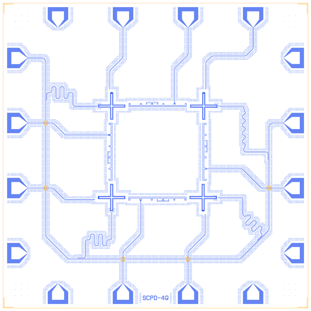
Eight benchmark chips (4 to 69 qubits) for automatic placement and routing of planar superconducting chips, from the MQT SCPD supplementary data (MIT). The GDS holds an abstract layout: qubits, couplers and launchers are obstacle blocks with named ports, and the routed file adds wire footprints. The notebook rebuilds the 4-qubit chip on the Quantcore PDK by putting a library component in every block and routing the connections of the routed benchmark; the other seven chips use the same block types and follow the same recipe.
This notebook is an example of turning an abstract placement into real parts: Xmons in the qubit blocks, metal:TunableCoupler01 in the coupler blocks, bond pads on the PDK pad rule, a feedline with 45° corners carrying four hanger readouts, and airbridges where control lines cross the feedline.
At a glance
Notebook |
|
Source |
|
Chip |
7.5 × 7.5 mm Quantcore die, the benchmark’s 6.9 × 6.5 mm launcher array centred in it, CPW 10 / 6 µm |
On the chip |
16 launchers (10 used) · 4 Xmons · 4 tunable couplers · 1 feedline · 4 λ/4 hanger readouts · 4 drive lines · 4 flux lines · 5 airbridges |
Builds today |
yes (layout built on 2026-11-19 in 11 s) |
How the notebook builds it
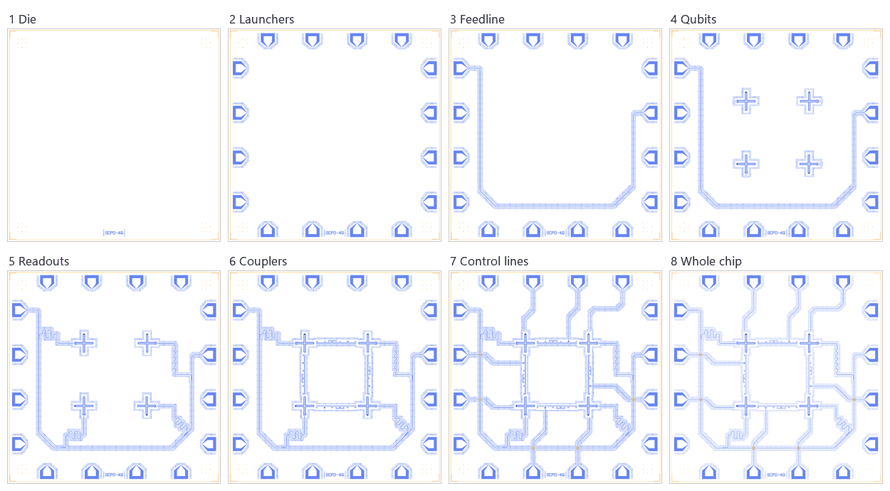
Die. The 7.5 mm die with the frame and the device ID
SCPD-4Q. Designer = source + (−101.54, +2176.71) µm puts the launcher array in the middle of the die.Launchers. 16
BondPads with the source’s 500 × 500 µm footprint, moved to the 100 µm pad rule (200 µm outward on the west and east edges, 400 µm on the north and south edges).Feedline. From
L0toL10on the corner points of the routed benchmark’s feedline, 13.74 mm.Qubits. Four
Xmons (620 µm tip to tip) at the centres of the qubit squares, each turned so that its junction arm faces the drive stub and its claw the readout tab.Readouts. Four λ/4 hangers at the source’s coupler positions (one of them on the 45° segment), 2425 / 2475 / 2525 / 2575 µm of wire plus a 200 µm coupled section.
Couplers. Four
metal:TunableCoupler01with a 1400 µm island and a PDK trilayer SQUID, and twelve declared capacitances (qubit to coupler, and qubit to qubit across each coupler).Control lines. Four drive lines to open ends at the drive stubs, four flux lines to the couplers’ flux pins, and a KQC airbridge at each of the five feedline crossings.
Whole chip. Five sim groups (one per qubit with its readout, and the
coreof qubits, couplers and drive ends), no centring shift, save.
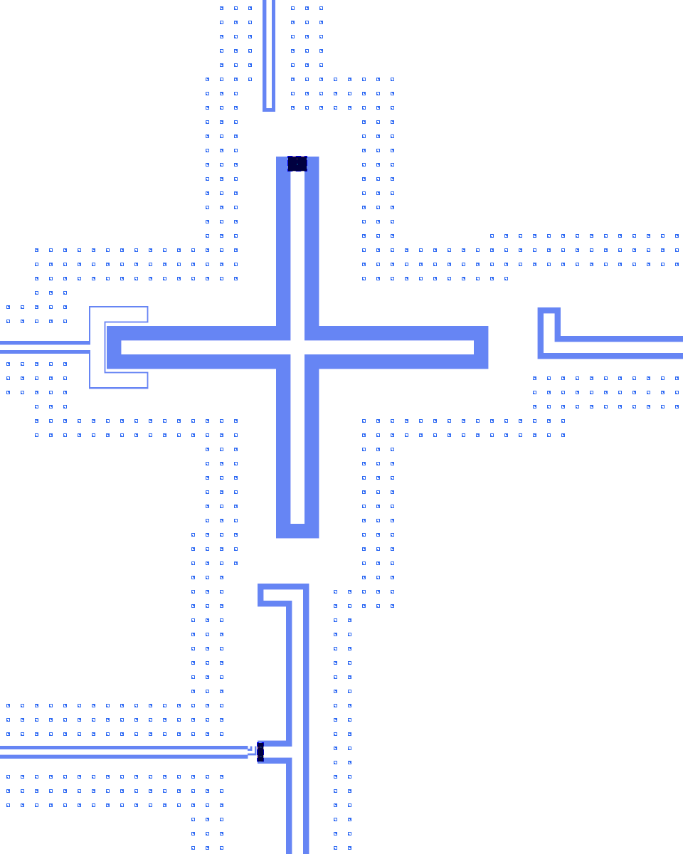
Q1 with its readout claw (left), the open drive end above its junction arm, the end of the C12 island (right) and the C14 island below, with its flux line.
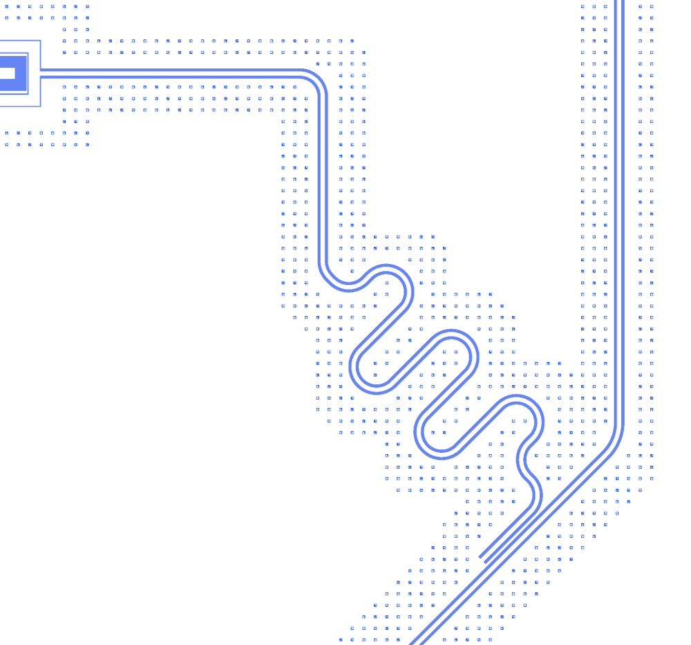
R3 meanders down to its hanger on the feedline’s 45° segment in the south-east corner.
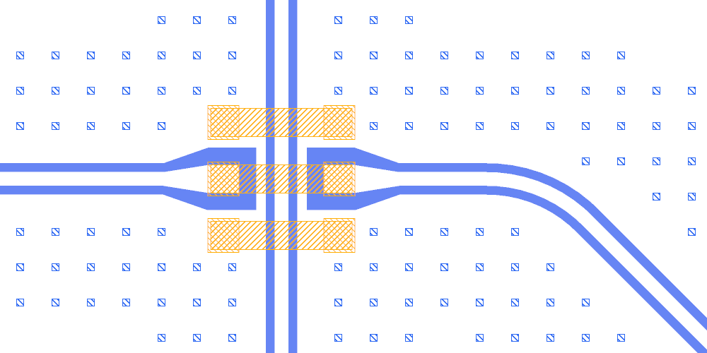
The C14 flux line crosses the west side of the feedline on a KQC airbridge.
LOM estimates
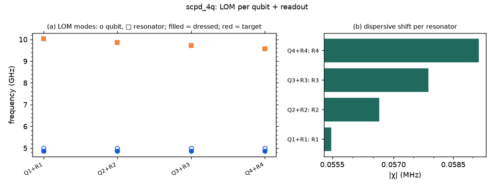
Numbers are from a run of this notebook on 2026-11-19 (Setup, Design, Check and the LOM cells, 32 s): QuCat normal modes with QuTiP dressed values, each qubit with its readout and the feedline.
group |
qubit |
f_q (GHz) |
α (MHz) |
resonator |
f_r (GHz) |
κ (MHz) |
χ (MHz) |
|---|---|---|---|---|---|---|---|
Q1+R1 |
Q1 |
4.866 |
-137 |
R1 |
10.03 |
0.234 |
-0.0555 |
Q2+R2 |
Q2 |
4.866 |
-137 |
R2 |
9.873 |
0.223 |
-0.0566 |
Q3+R3 |
Q3 |
4.866 |
-137 |
R3 |
9.719 |
0.214 |
-0.0579 |
Q4+R4 |
Q4 |
4.866 |
-137 |
R4 |
9.569 |
0.205 |
-0.0592 |
The four qubits are identical, so they share one frequency. The benchmark’s 2.5 mm λ/4 puts the readouts near 10 GHz, about 5 GHz above the qubits, so χ is small; the notebook keeps the benchmark’s length.
The coupler sweep (Q1–C12–Q2) steps the coupler’s SQUID L_J from its zero-flux 6.0 nH upwards. The coupler starts at 6.04 GHz, 1.2 GHz above the qubits. The effective coupling g̃ goes from +0.47 MHz at zero flux through zero at f_c ≈ 5.50 GHz (Φ ≈ 0.19 Φ0) to −2.2 MHz at 5.05 GHz, and the static ZZ of a detuned pair from +15 kHz through zero to −36 kHz. The couplings behind these numbers are rough estimates (1.4 fF from each qubit to the coupler, 0.06 fF between the qubits), and the coupler island’s capacitance is a rough one too (see the build spec), so the off point is only as good as they are.
L_J,c (nH) |
f_c (GHz) |
g̃ (MHz) |
ZZ (kHz), Q2 detuned |
|---|---|---|---|
6.00 |
6.045 |
0.465 |
15.3 |
7.00 |
5.583 |
0.114 |
3.06 |
7.25 |
5.483 |
-0.031 |
0.158 |
8.00 |
5.212 |
-0.817 |
-4.59 |
8.50 |
5.054 |
-2.24 |
-35.9 |
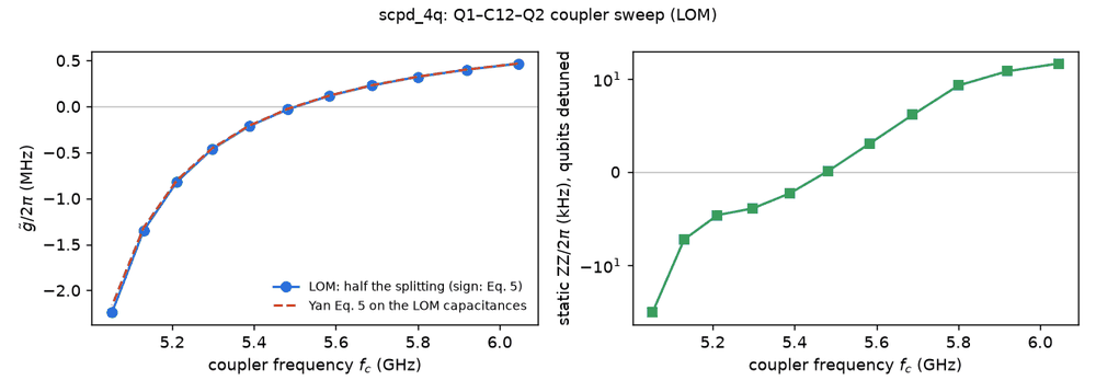
These are lumped-model estimates, not FEM results. The LOM page says how far to trust them.
Build spec
The rest of this page is the spec the notebook was built from: the source data, the eight chip families, and the 4Q blocks with the parts that replace them.
The source holds abstract blocks only, so the device geometry of any rebuild (qubit cross, coupler island, coupling gaps) is the rebuild’s own choice; metal:TunableCoupler01 is a stand-in for the tunable-coupler blocks.
Source: cda-tum/planar-superconducting-pd. Supplementary data
for Feldmeier, Walter, Huber, Bhattacharjee, Filipp, Wille, Physical Design Automation for Planar Superconducting
Quantum Chips (TCAD, under review). The tool is MQT SCPD.
Licence MIT (© 2026 MQT, verified). Read on 2026-11-02: README, inputs/*/config.toml, inputs/4q/routing_config.json,
and three small GDS files (4q unrouted and routed, 9q and 17q unrouted, ≤ 134 kB) parsed for block sizes. The
notebook’s numbers come from the 4q files read again on 2026-11-19 (config.toml, routing_config.json, both 4q GDS
files, qor/qor.csv), as data only.
What it is: eight benchmark chips for automatic routing. The GDS holds an abstracted layout: qubits, couplers and
launchers are obstacle blocks on 1/0. The routed GDS adds wire footprints on 2/0 (22 µm = 10 µm centre + 2 × 6 µm
gaps), 200 × 182 µm resonator–feedline coupler footprints on 3/0, airbridges on 4/0 and clearance zones on 5/0.
There is no qubit geometry, so a rebuild places catalog parts in the blocks. The notebook puts Quantcore Xmons in
the qubit blocks and metal:TunableCoupler01s in the 814 × 1420 µm coupler blocks (each with a flux port and two
bridge ports).
Chip families (from README Table I)
chip |
topology |
size (mm) |
launchers |
qubits = |W_r| resonators |
feedlines |
d_fix (µm) |
drive/flux wires |W_p| |
bridges |
|---|---|---|---|---|---|---|---|---|
4Q |
2 × 2 grid |
6.6 × 7 |
16 |
4 |
1 |
2500 |
8 |
5 |
9Q |
3 × 3 grid |
14.3 × 14.3 |
24 |
9 |
2 |
3000 |
21 |
15 |
17Q |
3 × 3 core + 8 boundary qubits |
14.3 × 14.3 |
48 |
17 |
4 |
3000 |
41 |
27 |
21Q |
X-shaped, 1 three-qubit block per corner |
24 × 24 |
72 |
21 |
5 |
4000 |
49 |
33 |
33Q |
X, 2 blocks per corner |
30 × 30 |
96 |
32* |
6 |
6000 |
78 |
57 |
45Q |
X, 3 blocks |
35 × 35 |
120 |
45 |
8 |
6000 |
105 |
82 |
57Q |
X, 4 blocks |
40 × 40 |
152 |
56* |
9 |
6000 |
134 |
101 |
69Q |
X, 5 blocks |
54 × 54 |
192 |
69 |
12 |
6000 |
163 |
121 |
* the table lists |W_r| = 32 and 56; the chip names say 33 and 57. Inner-region resonators are routed to d_fix + 3000 µm. Design rules (all chips): wire clearance 185 µm, obstacle clearance 25 µm, bend radius ≥ 50 µm, straight ≥ 100 µm, resonator length tolerance 100 µm, feedline capacity r_util 4–7 resonators.
4Q in detail (unrouted GDS, 1/0; rebuild: Designer = source + (−101.54, +2176.71), box (0, 0, 7500, 7500))
Block centres are the centres of the blocks’ bounding boxes in the source frame. A qubit block is a 680 × 680 µm square plus a 96 µm readout tab, so its square’s centre is 48 µm off the box centre; the rebuild puts each Xmon at the square’s centre and each coupler halfway between its two qubits.
block |
size (µm) |
box centre (source) |
rebuild part |
at (Designer) |
notes |
|---|---|---|---|---|---|
Q1 (north-west) |
776 × 680 |
(2724.2, 2790.1) |
|
(2670.66, 4966.81) |
ports in config: Qn.port0 (resonator, west here), Qn.port1 (drive, north) |
Q4 (south-west) |
680 × 776 |
(2772.2, 492.1) |
|
(2670.66, 2716.81) |
readout south, drive west |
Q3 (south-east) |
776 × 680 |
(5070.2, 540.1) |
|
(4920.66, 2716.81) |
readout east, drive south |
Q2 (north-east) |
776 × 680 |
(5084.3, 2789.2) |
|
(4934.76, 4965.91) |
readout east, drive north |
C14 / C23 (west / east) |
814 × 1420 |
(2667.7, 1664.4) / (5232.2, 1640.7) |
|
(2670.66, 3841.81) / (4927.71, 3841.36) |
Cnm.port0 = flux line; port1/port2 = bridge pair (a wire may cross) |
C12 / C34 (north / south) |
1420 × 814 |
(3921.5, 2984.1) / (3897.8, 330.0) |
same, rot 180° / 0° |
(3802.71, 4966.36) / (3795.66, 2716.81) |
same |
drive stubs |
182 × 330 / 330 × 182 |
4, 80 µm off the qubit squares |
|
the stubs sit 50 µm off the arm axis |
|
L0…L15 |
500 × 500 |
4 per side, 1600 µm pitch |
|
tips 600 µm from the die edges, at 1350 / 2950 / 4550 / 6150 µm along them |
Chip.port0…15 |
Routed 4Q: one feedline (chain of 5 p2p segments) carrying 4 λ/4 resonators of 2500 µm (coupler footprint
200 × 182 µm on the feedline). 8 launcher-to-port wires (4 drive + 4 coupler flux). 5 airbridges. Total p2p
wirelength 10.32 mm. 2 of the feedline chain ends go to launchers (launcher_target = 2).
wire |
from |
to launcher |
bridge |
|---|---|---|---|
feedline |
Chip.port0 |
Chip.port10 |
|
|
Q1.port1 |
Chip.port14 |
|
|
Q2.port1 |
Chip.port12 |
|
|
Q3.port1 |
Chip.port6 |
yes |
|
Q4.port1 |
Chip.port2 |
yes |
|
C12.port0 |
Chip.port13 |
|
|
C23.port0 |
Chip.port9 |
yes |
|
C34.port0 |
Chip.port5 |
yes |
|
C14.port0 |
Chip.port1 |
yes |
Chip.port3, port4, port7, port8, port11 and port15 are unused. In the rebuild the feedline is 13.74 mm and the eight control wires add up to 16.07 mm: the launchers sit 200–400 µm further out (PDK pad rule) and the lines run on to the drive ends and the flux pins inside the blocks, where the benchmark measures to the block edges.
LOM node structure (generic)
Each qubit couples to its NN tunable couplers (C, with flux line) and to one λ/4 readout resonator (d_fix). Each resonator hangs on one of |W_f| feedlines. Each qubit has a drive line. No qubit parameters are given; the rebuild uses the PDK nominal trilayer junction (R_n 45 kΩ) in the qubits and a PDK SQUID at 6.1 nH (parallel R_n 40.2 kΩ) in the couplers.
What the rebuild simplifies
The qubit cross, the coupler island and the coupling gaps are chosen to fill the blocks. The qubit–coupler and qubit–qubit capacitances are declared with
d.couplefrom coplanar-strip estimates; the Q3D jobcoremeasures them.The
TunableCoupler01LOM model estimates the island as a comb with c_width / 60 µm fingers (23 at 1400 µm, 86 fF), while the Metal cell draws six fingers on a bar of that length whatever c_width is. The coupler frequency of the LOM is therefore rough; thecorejob measures the island too.The routes follow the routed GDS’s corner points; the source’s 91 µm jog after Chip.port0 is left out, and the resonator paths are qcc meanders between two waypoints, not the source’s paths.
The benchmark gives all four resonators 2500 µm. The rebuild staggers them inside the 100 µm tolerance so the four readouts on one feedline differ in frequency.
The larger chips (≥ 21Q) have the same block types. The same recipe builds them: read the block centres from
layouts/unrouted/gds/<n>q_unrouted.gds(1/0; the files are 68–527 kB) and the wire corners from the routed GDS, and open the Designer on a die of the chip’s own size (the PDK frame is drawn on any box).