CapacitiveXCoupler
Capacitive coupler for testing FEM computations.
Source: KQC (KQCircuits). Category: coupler. Module: kqcircuits.elements.capacitive_x_coupler.
Warning
Legacy cell. KQC test element ‘for testing FEM computations’; unused. Ports p11..p41 and a LOM model since 2026-11-15
See also the catalog.
Pins
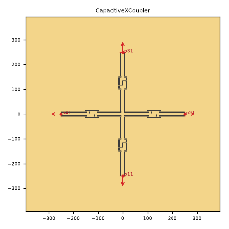
Pin image (default parameters). Light = metal, dark = etched gap, colours = junction layers. A red dot and arrow is a pin and its direction (out of the cell); the red bar is the CPW width a + 2 b. Blue dot = a pin without direction. Units: µm.
pin |
x (µm) |
y (µm) |
direction (°) |
a (µm) |
b (µm) |
purpose |
|---|---|---|---|---|---|---|
|
0 |
-250 |
270 |
10 |
6 |
LOM node |
|
250 |
0 |
0 |
10 |
6 |
LOM node |
|
0 |
250 |
90 |
10 |
6 |
LOM node |
|
-250 |
0 |
180 |
10 |
6 |
LOM node |
a, b: CPW centre width and gap where the pin declares them (– = not declared). Position and direction are in the cell’s own frame (at=(0, 0), rot=0).
Notes from the catalog: KQC draws no port refpoints, only its arm ends p11, p21, p31, p41 (KQC’s own simulation ports): qcc gives them as CPW ports (element a/b) facing out along each arm (registry.KQC_EXTRA_PORTS, ‘+’: S, E, N, W; ‘x’: the corners). LOM: each arm couples through its finger capacitor to the floating centre cross.
Parameters
name |
default |
unit |
description |
|---|---|---|---|
|
|
μm |
Width of center conductor |
|
|
μm |
Width of gap |
|
|
μm |
Turn radius |
|
|
– |
Length of Capacitive X Coupler |
|
|
– |
Height of Capacitive X Coupler |
|
|
– |
Coupler variant, either (+) or (x) |
|
|
– |
Remove capacitors from the X Coupler |
|
|
– |
Number of fingers |
|
|
μm |
Width of a finger |
|
|
μm |
Gap between the fingers |
|
|
μm |
Gap between the finger and other pad |
Electrically relevant parameters (sizes, gaps, junction, ports) come first, the rest follows.
LOM model
The cell contributes to the lumped model:
branch |
type |
nodes |
value (estimate at defaults) |
|---|---|---|---|
|
C |
p11 – c |
estimate=4.01, unit=fF, estimate_source=analytic: interdigital (Igreja & Dias 2004) + finger-tip gaps, as FingerCapacitorSquare, estimate_kind=analytic, uncertainty=±25% |
|
C |
p11 – gnd |
estimate=19, unit=fF, estimate_source=rough: 98 µm of arm CPW + half the finger block, estimate_kind=rough, uncertainty=±50% |
|
C |
p21 – c |
estimate=4.01, unit=fF, estimate_source=analytic: interdigital (Igreja & Dias 2004) + finger-tip gaps, as FingerCapacitorSquare, estimate_kind=analytic, uncertainty=±25% |
|
C |
p21 – gnd |
estimate=19, unit=fF, estimate_source=rough: 98 µm of arm CPW + half the finger block, estimate_kind=rough, uncertainty=±50% |
|
C |
p31 – c |
estimate=4.01, unit=fF, estimate_source=analytic: interdigital (Igreja & Dias 2004) + finger-tip gaps, as FingerCapacitorSquare, estimate_kind=analytic, uncertainty=±25% |
|
C |
p31 – gnd |
estimate=19, unit=fF, estimate_source=rough: 98 µm of arm CPW + half the finger block, estimate_kind=rough, uncertainty=±50% |
|
C |
p41 – c |
estimate=4.01, unit=fF, estimate_source=analytic: interdigital (Igreja & Dias 2004) + finger-tip gaps, as FingerCapacitorSquare, estimate_kind=analytic, uncertainty=±25% |
|
C |
p41 – gnd |
estimate=19, unit=fF, estimate_source=rough: 98 µm of arm CPW + half the finger block, estimate_kind=rough, uncertainty=±50% |
|
C |
c – gnd |
estimate=74, unit=fF, estimate_source=rough: inner arm CPW sections + half finger blocks, estimate_kind=rough, uncertainty=±50% |
Nodes: c, p11, p21, p31, p41.
Simulation export notes
C7: C-matrix nets without a design label (warning) (status: fixed; fix in sim_tools/builder.py (_cell_probes, label_unnamed); layouts/others/amplifiers.py (JtwpaChain.qcc_probes))
How to use
In Python:
from quantcore_circuits.designer import Designer

d = Designer("demo", box=(0, 0, 7500, 7500))
d.add("U1", "CapacitiveXCoupler", at=(3750, 3750), a=10)   # parameters: see the table above
d.add("PAD", "BondPad", at=(1125, 3750), rot=270)   # a launcher to connect to
d.route("L1", "PAD.a", "U1.p11")                # a CPW from the pad to the pin
Pin names go into d.route(...) as INSTANCE.pin, and into snap= / to= when placing. From the shell: qcc components CapacitiveXCoupler lists the pins; add --schema for the parameters.
In KLayout: Quantcore panel ▸ Components ▸ double-click the cell, then click on the layout to place it. Rotate and mirror before the click; use Connect on two pins to route.