Compact junction cell (chip_11m)
Not a full chip but the unit cell of a junction test array: one trilayer junction in a 12 × 12 µm exposure window, made of a straight finger, a bent finger and two small HSQ boxes. The cell is meant to be repeated across a wafer to measure junction resistance against size. The script also defines two probe pads but never draws them.
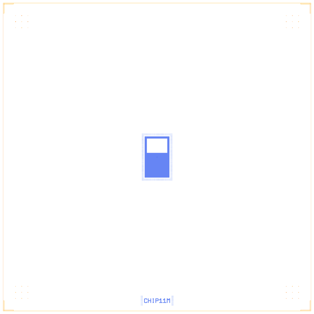
It comes from Quantcore’s QWri script chip_11m_TestJJ16x_pads.py (internal; chip_11f places the same cell). The rebuild puts one 0.5 × 0.6 µm junction on a probe-pad pair in the middle of an otherwise empty PDK die (device ID CHIP11M), valued at 45 kΩ on the PDK junction rule. Build it to see the smallest repeatable unit of the junction chips.
At a glance
Notebook |
|
Source |
Quantcore legacy QWri script |
Chip |
7.5 × 7.5 mm Quantcore die, sapphire |
On the chip |
1 |
Builds today |
yes, rebuilt from its JSON on 2026-11-19 in 0.9 s (the notebook itself was not re-run) |
Pictures
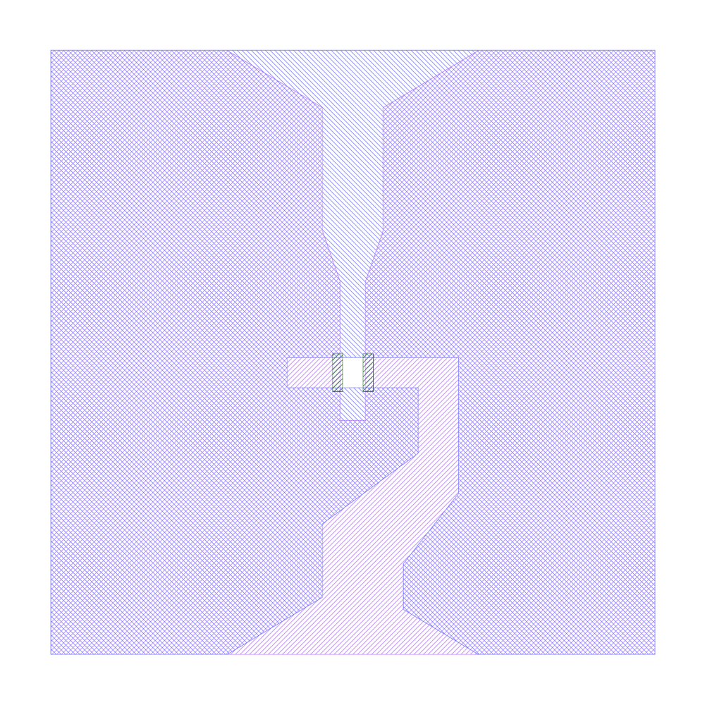
The original legacy layout (render of the legacy GDS), a close view of the junction at the centre.
The rebuild: one probe-pad pair at the die centre.
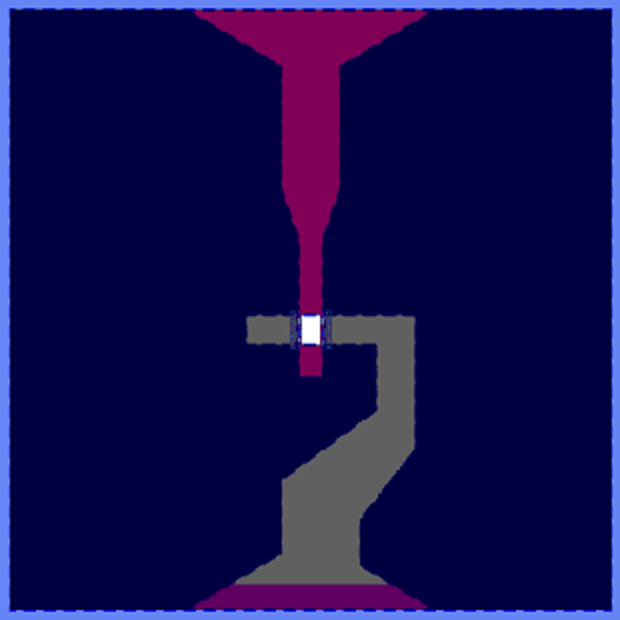
The junction window at the centre (a 40 µm view), where the two fingers meet.
LOM estimates
The notebook has no saved LOM output. The chip has no qubit or resonator, so its LOM netlist is empty.
Build spec
The rest of this page is the detailed spec the notebook was built from: every component, the changes made while rebuilding, and the notes.
Source: components/python/chip_11m_TestJJ16x_pads.py (create_testPad(size, secondFinger), writes
chip_11m_jnc<size>_<secondFinger>.gds with one cell JX_500; __main__ calls create_testPad(2.5, 0.6)). Legacy
QWri library, Quantcore internal. Notebook examples/designs/legacy/chip_11m_testjj16x_pads.ipynb.
Changes made in the rebuild
Junctions:
JX(0.5 × 0.6 µm) on the PDK junction rule (Nb trilayer, Δ = 1.4 meV, I_c·R_n = πΔ/2e = 2.20 mV, R_n 40–50 kΩ, qubits 4–8 GHz; PDK processget_pdk().junction: R_n·A 13.5 kΩ·µm², C_J 50 fF/µm², both assumed by the PDK): 45 kΩ; chip_11f’s JX_500 (0.2 × 0.6 µm) 112.5 kΩ.The notebook’s JSON was rebuilt from its layout cell. The notebook has not been re-run, so its outputs are cleared and its PNGs may be out of date.
What it is: the unit cell of a junction test array, not a full chip (“this is the unit cell which will be
scaled”; “creates the junction in-house, without the junction_creator”). One trilayer junction in a 12 × 12 µm
exposure window: a straight finger (JJ_finger Top, mirrored, 1.2 µm lead) on 2/0, a bent finger (JJ_finger Bottom, 1.6 µm lead) on 4/0, two 0.2 µm HSQ boxes on 500/0, and a triangular notch cut from each finger window
where its lead meets the window edge. The script defines two 500 × 400 µm probe pads and a 600 × 1000 µm window but
never inserts them (only the junction is drawn); the pads it is meant for are patterned elsewhere (not in the
library). chip_11f_JJplacer.py places this cell, built with create_testPad(1.0, 0.6), at external coordinates
(see chip_11f_jjplacer.md). The script declares the gradient layers 52/53/54 but draws none.
Builds: yes. TrilayerJunctionCompact (the port of JX_500, golden test
test_trilayer_junction_compact[1.0-0.6 / 2.5-0.6]).
Components (legacy frame)
instance |
legacy cell → catalog ref |
params |
at |
notes |
|---|---|---|---|---|
JX |
|
straight finger |
legacy window centre (0, 0) → Designer (3750, 3750); the cell’s origin is its window’s lower edge, so |
the |
No die in the source (it writes the bare cell). Rebuilt on the PDK v2 die frame (the Quantcore chips), the cell at the
die centre, with the device ID CHIP11M.
Routes, test pads, LOM
No routes, no pads. LOM: TrilayerJunctionCompact’s model is one JJ branch J_JX from JX.j (port common, the
lead that lands on the separately patterned pad) to ground; common is listed as unconnected (nothing in this
source attaches to it). Junction values from the area (0.5 × 0.6 µm², assumed Jc: to be confirmed). “LOM
simulation” = the junction table (this cell, and the size-1.0 variant chip_11f places). No sim groups, no FEM jobs.
Keep-outs
None: a 12 µm cell at the die centre.