Two coupled transmons (Metal A.2)
Two pocket transmons joined by an 8 mm bus resonator, each read out by its own λ/4 resonator on one shared feedline. It is the Qiskit Metal “A.2” full-design example (Apache-2.0, © IBM and contributors), adapted from the SQDMetal benchmark devices. The Quantcore rebuild is distributed under GPL-3.0.
Build this one to learn the two-qubit gate building block, with two readout resonators of different length on a single feedline and a coupler bus between the qubits. It also shows how the PDK puts the two bond pads 100 µm from the die edge.
At a glance
Notebook |
|
Source |
Qiskit Metal |
Chip |
14 × 9 mm (the source’s size, larger than the 7.5 mm Quantcore die), CPW 10 / 6 µm |
On the chip |
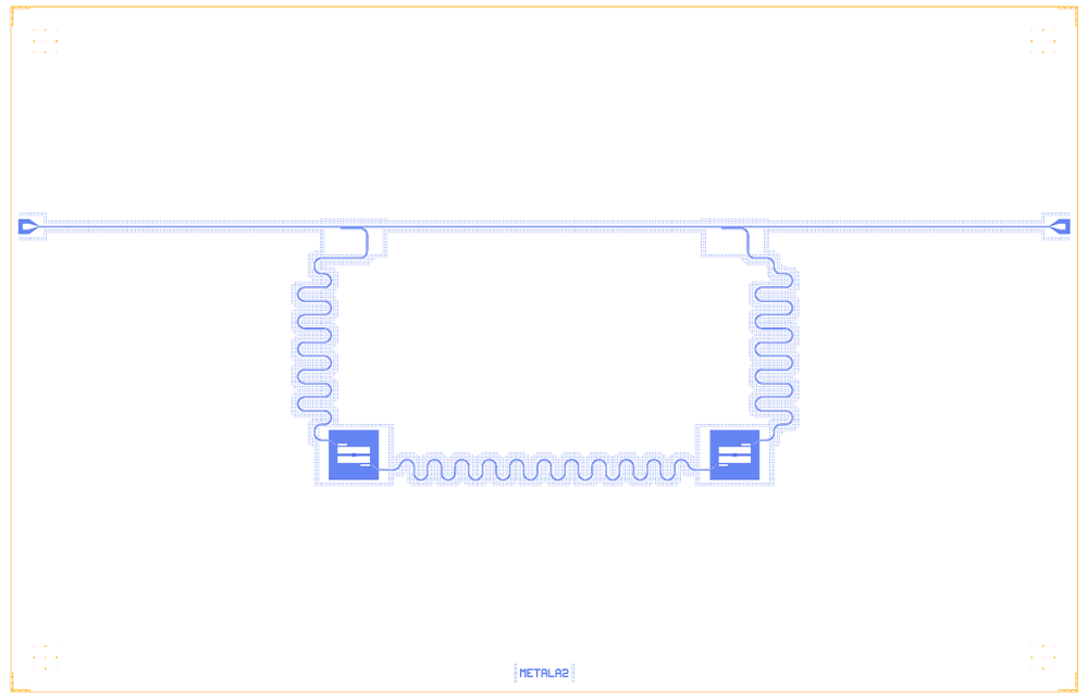
2 pocket transmons · 2 λ/4 readouts (7.0 and 7.2 mm) · 2 coupled-line tees · 1 feedline · 1 λ/2 bus (8 mm) · 2 bond pads |
Builds today |
yes (layout built on 2026-11-19 in 10 s) |
How the notebook builds it
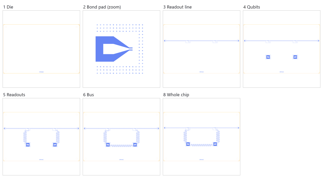
Die. An empty 14 × 9 mm chip with the QCT frame (dicing marks, alignment grids, chip boundary, device ID).
Bond pads. Two launchpads, slid to the 100 µm pad-edge rule (the picture zooms on one pad).
Readout line. Two coupled-line tees on the feedline, one above each qubit.
Qubits. Two Metal pocket transmons with Quantcore junctions, each with a readout pad and a coupler pad.
Readout resonators. A 7.0 mm and a 7.2 mm λ/4 meander from the tees to the qubits.
Coupling. An 8 mm λ/2 bus between the two coupler pads.
Control lines. None; the qubits are driven and read through their readouts.
Whole chip. Sim groups for the FEM jobs, the content centred in the die, the design saved.
LOM estimates
Numbers are from a run of this notebook on 2026-11-19 (Setup, Design, Check and the LOM cells, 12 s): QuCat normal modes with QuTiP dressed values.
group |
qubit |
f_q (GHz) |
α (MHz) |
resonator |
f_r (GHz) |
κ (MHz) |
χ (MHz) |
|---|---|---|---|---|---|---|---|
Q1+read1 |
Q1 |
7.218 |
-322 |
clt1 |
3.929 |
0.0896 |
-0.292 |
Q2+read2 |
Q2 |
7.218 |
-322 |
clt2 |
3.833 |
0.0833 |
-0.254 |
group |
pair |
ZZ (kHz) |
neighbours |
hybridised |
|---|---|---|---|---|
Q1+Q2+bus |
Q1-Q2 |
– |
yes |
yes |
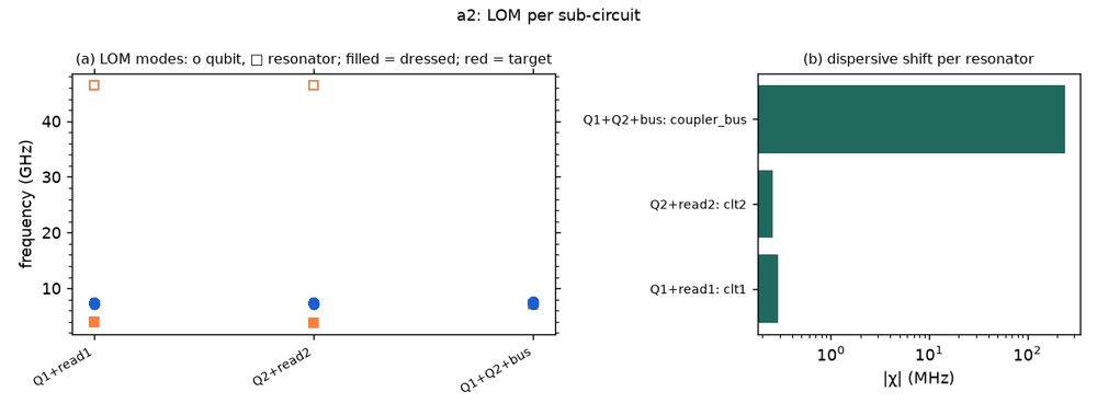
These are lumped-model estimates from component formulas and calibration, not FEM results. The LOM page says how far to trust them.
Build spec
The rest of this page is the detailed spec the notebook was built from: every component, port, route and length.
The
metal:references in this spec build as written, through themetal:wrapper (ports are the Metal pin names, parameters the Metal options). The Quantcore and KQC substitutions are optional.
Source: Quantum Metal docs/tut/full-design-examples/A.2-Two-coupled-transmons.ipynb. Licence Apache-2.0. It is
adapted from the SQDMetal benchmark devices (Sommers et al., arXiv:2511.01220, 2025).
The chip has two TransmonPocket qubits, each with a readout pad (top, outward) and a coupler pad (bottom, inward).
Two λ/4 readouts of different length hang off one feedline through CoupledLineTees, and an 8 mm meandered bus joins
the two coupler pads. This is the two-qubit gate building block.
Chip 14 000 × 9000 µm, centred, so Designer = Metal + (7000, 4500). CPW 10/6 µm, fillet 90 µm.
A first build uses these substitutions: Xmon (2 claws) for TransmonPocket, hangers for the CoupledLineTees, BondPad.
Components
instance |
catalog ref |
key params (µm) |
at (x, y) |
rot |
notes |
|---|---|---|---|---|---|
Q1 |
|
Metal pad_width 425, pocket_height 650; readout (loc_W −1, loc_H +1), coupler (+1, −1), default pad 125 × 30 |
(4500, 3000) |
0 |
claw_n = readout (Metal pin (4075, 3195) W); claw_e = coupler (Metal (4925, 2805) E) |
Q2 |
|
readout (+1, +1), coupler (−1, −1) |
(9500, 3000) |
0 |
claw_n = readout (Metal (9925, 3195) E); claw_w = coupler (Metal (9075, 2805) W) |
clt1, clt2 |
hangers on FL (metal:CoupledLineTee) |
coupling_length 350, space 3, down_length 300, short |
centres (4500, 6000), (9500, 6000) |
0 |
legs at x + 175 |
LP1 |
|
(1025, 6000) |
270 |
faces E |
|
LP2 |
|
(12975, 6000) |
90 |
faces W |
Routes
route |
from → to |
type, length |
waypoints / hanger |
notes |
|---|---|---|---|---|
FL |
LP1.a → LP2.a |
cpw 11 950 |
— |
Metal feed_L 3125 + tee + feed_M 4300 + tee + feed_R 3125 |
read1 |
Q1.claw_n → |
meander 7650 |
— |
Metal 7.0 mm + 650 tee |
read2 |
Q2.claw_n → |
meander 7850 |
— |
Metal 7.2 mm + 650 tee |
coupler_bus |
Q1.claw_e → Q2.claw_w |
meander 8000 |
— |
λ/2 bus; Metal lead 150/150, asym 200 |
Launchers, pads, test structures, markers, labels
2 pads (W/E). There are no markers.
LOM node structure
Q1 and Q2 are transmons. Each has C_g to its own λ/4 readout (R1 7.65 mm, R2 7.85 mm, so about 100 MHz apart), and each readout has a κ to the shared FL between two 50 Ω ports. A λ/2 bus (8 mm) carries C_g to both qubits. There are no control lines.
Targets (if stated)
None. Estimates: readouts ≈ 4.1 / 4.0 GHz and bus ≈ 7.9 GHz on sapphire (all λ/4 or λ/2 estimates).
Simplifications for a first rebuild
Xmon claws: readout up (claw_n), coupler toward the neighbour (claw_e on Q1, claw_w on Q2). The Metal pads sit on the pocket corners; the Xmon puts them on the axes.
Build one FL with two hangers. This is the next step after
A1_transmon_readout.
Quantcore PDK rebuild
The notebook is a Quantcore PDK rebuild of the source, not a replica: the netlist, LOM and imported components are kept, and the process is Quantcore’s.
Notebook: examples/designs/metal/a2_two_coupled_transmons.ipynb.
Chip: the Quantcore die frame (L dicing markers 1000/0, 3 × 3 alignment grids 1001/0, chip boundary 100/0, device ID where an edge is free; any brand text is QCT), drawn on the source’s 14 × 9 mm chip (the design does not fit the 7.5 mm die); no KQC chip frame.
Stack: sapphire 650 µm, εr 10.25 (the PDK default stack, used by the LOM estimates and every FEM export); Metal’s
DesignPlanardefault is silicon (εr 11.45, 750 µm), so the LOM capacitances, resonator frequencies and FEM jobs here are for sapphire rather than the source’s substrate.Junctions: Quantcore Nb/AlOx/Nb trilayer junctions (
junction_typefromlayouts.registry.trilayer_junction): fingers on 2/0 + 4/0, spacer 50/0 with the 51–53/0 gradient, sized on the PDK junction rule (Nb Δ = 1.4 meV, I_c·R_n = πΔ/2e, R_n·A 13.5 kΩ·µm² and C_J 50 fF/µm² assumed); both qubits get the PDK nominal junction, 0.5 × 0.6 µm fingers → R_n = 45 kΩ, L_J = 6.73 nH, C_J = 15 fF (in the 40–50 kΩ window), in place of Metal’shfss_inductance10 nH (+ 2 fF assumed). Expected f_q ≈ 7.2 GHz (an estimate from the LOM). The two qubits stay identical, so the bus still hybridises their modes and the per-pair ZZ is not defined (section 4).Kept: the topology and every Metal component with the source’s options (through the
metal:wrapper), positions and orientations, every route’s end pins and total length, the sim groups (readouts 7.0 / 7.2 mm, the 8 mm bus).