Hyperbolic lattice chip (QPDK)
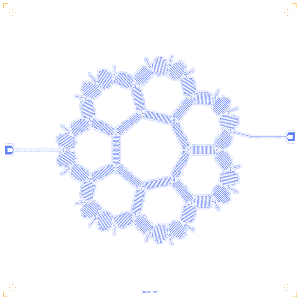
A finite flake of the {7,3} hyperbolic tiling drawn as a lattice of CPW resonators: 42 edge resonators of 7500 µm, each meandered inside its own region, meeting at 35 three-pin capacitive couplers, with shorted stubs on the free boundary pins and two probe lines. The layout comes from QPDK’s hyperbolic_lattice_chip.py (MIT, © 2024 gdsfactory), after Kollár et al., Nature 2019, and is rebuilt on the Quantcore PDK: sapphire, the QCT die frame, launchers 100 µm from the die edge. The rebuild is GPL-3.0. The chip has no qubits.
This notebook is an example of a layout computed from a formula (the tiling in the Poincaré disk), of ports at arbitrary angles (coupler pins along the geodesic tangents), of exact-length meanders drawn through your own nodes (nodes= together with meander=), and of the LOM of a resonator lattice.
At a glance
Notebook |
|
Source |
gdsfactory |
Chip |
14 × 14 mm: the 6000 µm-radius disk of the tiling, centred, plus the launchers; CPW 10 / 6 µm |
On the chip |
2 launchers · 35 vertex couplers · 42 edge resonators (7500 µm each) · 19 shorted stubs · 2 probe lines |
Builds today |
yes (layout built on 2026-11-19 in 41 s) |
How the notebook builds it
Before the layout the notebook computes the tiling: the central heptagon’s corners at Poincaré radius 0.3007, the shell by reflecting it across each edge (inversion in the edge’s geodesic circle), the pin of each edge along its geodesic tangent (exactly 120° apart at every vertex, because the disk model is conformal) and QPDK’s vertex numbering.
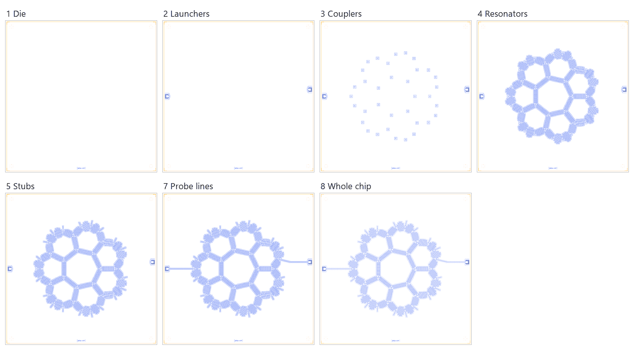
Die. The 14 × 14 mm die with the frame and the device ID.
Bond pads. Two launchers on the 100 µm pad rule: P1 on the west edge, P2 on the east edge.
Couplers. 35
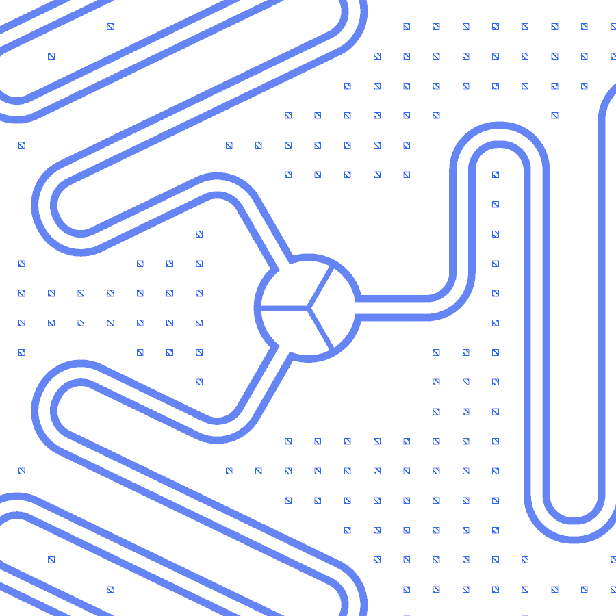
HyperbolicVertexCouplers at the vertices, pins along the geodesic tangents (the chip has no qubits).Resonators. 42 edge resonators of 7500 µm, each a serpentine inside its region, drawn with
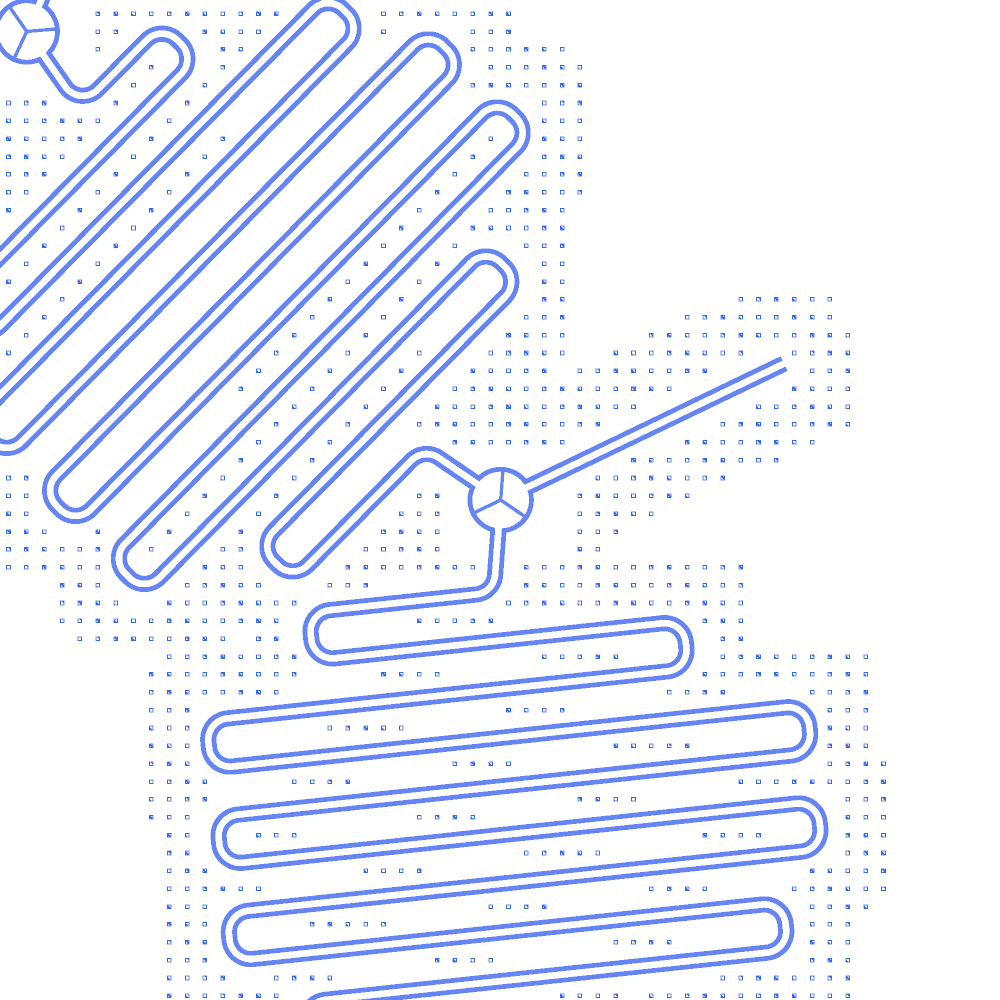
nodes=andmeander=7460.Stubs. 19 shorted 400 µm stubs on the free boundary pins.
Coupling. Nothing to add: the couplers are the coupling.
Probe lines. F1 straight west from free pin 11, F2 from free pin 0 with one 13.5° turn onto the x axis.
Whole chip. Two sim groups (the central coupler, one central resonator), the centring check, save.
The two zooms show the central coupler V0 with the ends of its three resonators, then vertex 9 on the rim with its shorted stub between two rim resonators.
LOM estimates
Numbers are from a run of this notebook on 2026-11-19 (Setup, Design, Check and the LOM cells, 84 s). All 42 resonators have the same length, so the same bare frequency: the λ/2 of 7460 µm on sapphire, 8.447 GHz. Loaded by its two couplers each one sits lower. One resonator with its two couplers per group (QuCat normal modes):
group |
edge |
f_r (GHz) |
κ (MHz) |
|---|---|---|---|
R0 |
central |
8.1197 |
0 |
R11 |
radial |
8.1197 |
0 |
R10 |
outer, one end at a stub |
8.1055 |
0 |
R9 |
rim, both ends at stubs |
8.0914 |
0 |
R7 |
outer, one end at the east probe |
8.1057 |
1.72 |
R8 |
rim, at the east probe and a stub |
8.0915 |
1.71 |
In these one-resonator cuts the other pins of an interior coupler float, while a stub or the 50 Ω probe pulls a free pin close to ground and loads that end more; that is the 28 MHz spread. A stub and a probe load a pin about equally.
The lattice. QuCat does not solve the whole lattice: the flake’s sevenfold symmetry makes most of its modes come in degenerate pairs, and QuCat finds none of them (on the central heptagon alone it returns no mode and simulate stops). The notebook therefore solves the same LOM circuit (d.lom() with the component estimates) as a lossless normal-mode problem, each resonator as the LC of its fundamental. The 42 modes span 7.997–8.216 GHz and follow the tight-binding band f₀ + t·λ of the line graph, with f₀ = 8.075 GHz and t = 39.3 MHz (rms residual 0.7 MHz). The seven lowest modes are the flat band at 7.9968 GHz (spread 6 kHz, f₀ − 2t = 7.996 GHz): the line graph has the eigenvalue −2 seven times (E − V = 42 − 35). The flat band sits at the bottom of the band, at ω₀ − 2|t| as QPDK describes it. The 19 stubs resonate at 59.7–59.8 GHz, far above the band. Widening every coupler’s pin gap from 4 to 8 µm (LOM 3 of the notebook) lowers t to 34.1 MHz and lifts the flat band to 8.029 GHz.
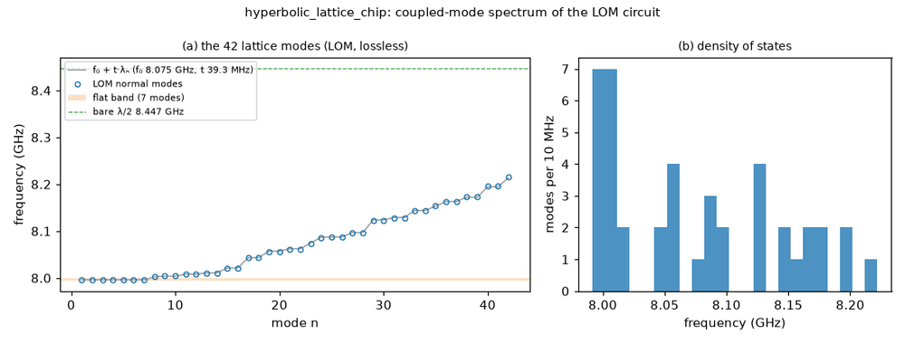
These are lumped-model estimates (component formulas and calibration), not FEM results; the coupler capacitances are rough estimates (±50 %), so t is the least certain number. The LOM page says how far to trust them.
Build spec
The rest of this page is the spec the notebook was built from, with what the build settled.
Source: qpdk/samples/hyperbolic_lattice_chip.py
· generator qpdk/cells/hyperbolic.py (hyperbolic_lattice, hyperbolic_edge_resonator, hyperbolic_vertex_coupler)
and tiling maths qpdk/hyperbolic.py · licence MIT (verified). No image of the chip in the repo.
Reference: Kollár et al., Hyperbolic lattices in circuit QED, Nature 2019 (kollarHyperbolicLatticesCircuit2019).
What it is: a finite flake of the {p, q} = {7, 3} hyperbolic tiling (central heptagon + shells = 1 ring) mapped from
the Poincaré disk onto a 6000 µm-radius disk on chip. Every tiling edge is one CPW resonator of exactly 7500 µm
(pin rim to pin rim), meandered inside the quadrilateral formed by its two vertices and the centroids of the two
adjacent faces. Every vertex is a 3-pin capacitive disk coupler. Free boundary pins get a 400 µm shorted λ/4 stub
(far above the band). Two free pins (probe_pins = (11, 0)) are fed out to launchers. The model is line-graph tight
binding with t < 0 and a flat band at ω₀ − 2|t| (QPDK’s description).
Size: the source frames the lattice’s bounding box with a 500 µm edge_margin. The rebuild uses a 14 × 14 mm die,
box (0, 0, 14000, 14000), disk centre at (7000, 7000): the 6000 µm disk plus the launchers on the pad rule. The flake
itself reaches 4164 µm from the centre (about 4.6 mm with its stubs).
Generator (the tiling, not a per-instance table)
item |
count (derived for {7,3}, 1 shell) |
parameters |
|---|---|---|
faces (heptagons) |
8 (1 central + 7) |
the central heptagon’s corners at Poincaré radius r₀ = tanh(R/2), cosh R = cot(π/7) cot(π/3) (r₀ = 0.3007, QPDK |
vertices = couplers |
35 (14 interior/degree-3, 21 boundary/degree-2) |
pin_radius 40, pin_gap 4 (radial), ground_gap 6, lead_length 20; one pin per incident edge, oriented along the geodesic tangent |
edges = resonators |
42 |
length 7500 µm rim-to-rim (leads included), bend_radius 30, margin 25 µm from region edge, end_straight 70 |
boundary stubs |
21 free pins − 2 probes = 19 |
shorted CPW, 400 µm pin-rim to short |
probe lines |
2 (free pins 11 and 0) |
F2: 1000 µm along the pin direction, then onto the +x axis; F1: straight (its pin points along −x) |
The counts are derived from the tiling (V − E + F = 35 − 42 + 8 = 1 for the disk); the notebook’s own tiling gives the same. Vertex positions: the tiling in the unit disk, scaled by 6000 µm, around the die centre. The notebook numbers the vertices as QPDK does (central heptagon first with a corner on +x, then each outer heptagon, each vertex where it is first reached), so free pins 0 and 11 are QPDK’s probe pins: free pin 11 is vertex 23 on the −x axis (pointing 180°), free pin 0 is vertex 8 (pointing 346.5°). Chords on the chip: 1566 µm (central edges), 1390 µm (radial), 1097 µm (outer), 933 µm (rim); the pins deviate from the chords by up to 10.4°.
Components
instance |
catalog ref |
key params |
at |
rot |
notes |
|---|---|---|---|---|---|
V0…V34 |
|
q 3, pin_radius 40, pin_gap 4, ground_gap 6, lead_length 20, |
tiling vertex × 6000 µm + (7000, 7000) |
0 (the cell’s |
a 40 µm-radius metal disk cut into 3 pie-slice pins by 4 µm radial gaps, 6 µm ground ring, each pin feeds a 20 µm CPW lead; ports |
P1 |
|
QPDK launcher size ( |
west edge, y 7000 |
270 |
launcher 1 (free pin 11), 100 µm from the die edge ( |
P2 |
|
same |
east edge, y 7631 (the height of F2’s corner) |
90 |
launcher 2 (free pin 0), 100 µm from the die edge |
Routes
route |
from → to |
type, length |
notes |
|---|---|---|---|
R0…R41 |
V_i.o_k → V_j.o_l |
meander 7460 port to port, r 30 (7500 rim to rim with the 2 × 20 µm leads) |
a serpentine computed in the notebook inside the edge’s region (the two vertices and the adjacent face centroids; for boundary edges the outer apex is the mirrored centroid × 0.6), 25 µm margin, legs at least 62 µm apart, 70 µm end straights; drawn with |
S_v (19) |
V_v.free pin → free_end (short) |
cpw 380 (400 from the pin rim) |
λ/4 stub |
F1 |
V23.o2 → P1.a |
cpw, straight west |
free pin 11 |
F2 |
V8.o2 → P2.a |
cpw, 1000 µm along the pin, then onto +x |
free pin 0 |
LOM node structure
42 identical λ/2 CPW resonators (7460 µm port to port, 8.447 GHz bare on sapphire) as nodes of the line graph: in the LOM a meandered route between
two coupler ports is one λ/2 TLres whose two end nodes join into one resonator node. Each vertex coupler is a
capacitance network between the three resonator ends that meet there (pin–pin across the 4 µm gap, pin–ground across
the ring; the cell’s rough estimates). 19 shorted λ/4 stubs load the free boundary pins. Two 50 Ω probe ports. No
qubits, no control lines.
Targets
None numeric. The design goal is identical hopping t on every coupler and identical ω₀ on every resonator. The notebook’s feedback cells use an exercise target on a copy (the flat band at 8.10 GHz).
What the build simplified
The serpentine is computed in the notebook (legs perpendicular to the line between the two end straights, U-turns capped by the region’s room and by one common height solved for the length) and drawn with
nodes=andmeander=7460; the router closes the last 2 µm by trimming the corner radii. Its legs are at least 62 µm apart (QPDK: 60 µm), so a U-turn’s two r = 30 µm bends pass the router’s bend check.QPDK clips each boundary region’s outer apex at the bisector with the next boundary edge; on this flake no apex reaches it, so the notebook leaves the clip out (the DRC is clean without it).
The launchers are
BondPads on the PDK pad rule, so F1 runs straight from its pin to the west edge and F2 keeps QPDK’s corner 1000 µm along its pin, then runs east to its pad; both are longer than QPDK’s feeds.The LOM spectrum of the whole lattice comes from a lossless normal-mode solve written in the notebook (the same LOM circuit), because QuCat does not solve the degenerate lattice; QuCat gives the one-resonator groups.
Quantcore PDK rebuild
The notebook is a Quantcore PDK rebuild, not a replica: the topology, sizes and lengths are the source’s, the process is Quantcore’s.
Chip: the Quantcore die frame (L dicing markers 1000/0, 3 × 3 alignment grids 1001/0, chip boundary 100/0, the device ID QPDK-HYP; any brand text is QCT) on a 14 × 14 mm die that holds the 6000 µm disk and the launchers.
Stack: sapphire 650 µm, εr 10.25 (the PDK default stack, used by the LOM estimates and every FEM export); QPDK’s process is Al on Si (εr 11.45), so frequencies are not the QPDK ones.
Junctions: none on this chip.
Cheese: the PDK band around the components (the source has none).
Sim groups:
V0(Q3D C-matrix of the central coupler) andR0(eigenmode, and a driven run, of one central resonator with its two couplers); the whole lattice is too large for one FEM job.Kept: the tiling and its numbering, the coupler geometry, the 7500 µm resonators and their regions, the stubs, the probe pins.