TSV flip-chip test chip (QPDK)
A QPDK interconnect test chip for a two-chip stack: two mirrored CPW lines that pass through all four metal faces, using through-silicon vias (TSVs) on both chips and an indium-bump transition between them. It has no resonators and no qubits. The layout comes from QPDK’s tsv_flip_chip_test_chip.pic.yml (MIT, © 2024 gdsfactory) and is rebuilt on the Quantcore PDK; the rebuild is GPL-3.0.
This notebook shows how a line moves between KQC’s four faces in one design. CpwTsvTransition and QcFlipChipConnectorRf record the face of each of their ports, every route is drawn on the face of the port it starts on, the DRC checks each face on its own, and the sim groups are exported on the faces they join. It also shows what the PDK fab map does with faces it has no layer for.
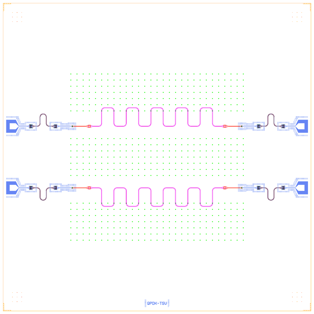
At a glance
Notebook |
|
Source |
gdsfactory |
Chip |
10 × 10 mm bottom chip with the Quantcore die frame, the 6 × 6 mm top chip over its centre (not drawn), CPW 10 / 6 µm on four faces |
On the chip |
4 launchers · 2 through lines · 12 TSV transitions (8 on the bottom chip, 4 on the top chip) · 4 bump transitions · 609 ground bumps |
Builds today |
yes (layout built on 2026-11-19 in 15 s) |
How the notebook builds it
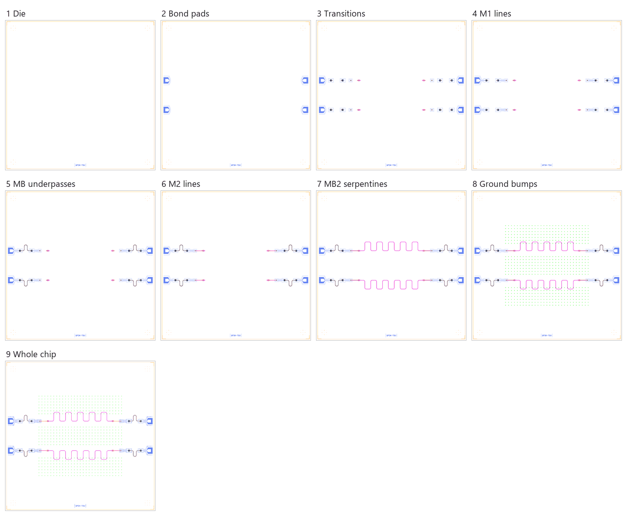
Die. The 10 × 10 mm Quantcore die with the frame and the device ID QPDK-TSV.
Bond pads. Four launchers on the front face, 100 µm from the die edge (where QPDK already puts them).
Transitions. Twelve
CpwTsvTransitions (eight through the bottom chip, four through the top chip) and fourQcFlipChipConnectorRfbumps between the chips.M1 lines. On the bottom chip’s front: the feed lines from the launchers and the lines to and from the bumps.
MB underpasses. Four loops on the bottom chip’s back between the down and up transitions.
M2 lines. On the top chip’s front: from the bumps to the top chip’s TSV transitions.
MB2 serpentines. Two ten-leg serpentines on the top chip’s back, between its two TSV transitions.
Ground bumps. Three 29 × 7 arrays of indium bumps, 609 in all, between the two front faces.
Whole chip. Three sim groups, the centring check (no shift), the save, and a picture of each face on its own.
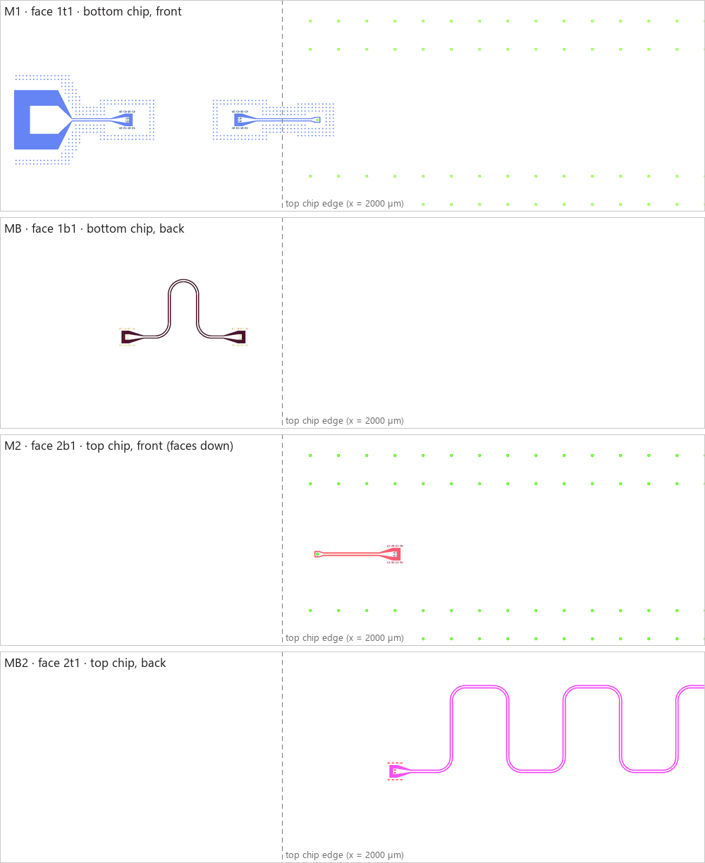
The four faces of the west half of line a, one at a time. The line leaves the launcher on M1, goes through the bottom chip to its back (MB) for the underpass and comes back to M1, crosses to M2 at the bump just inside the top chip, and goes through the top chip to its back (MB2) for the serpentine:
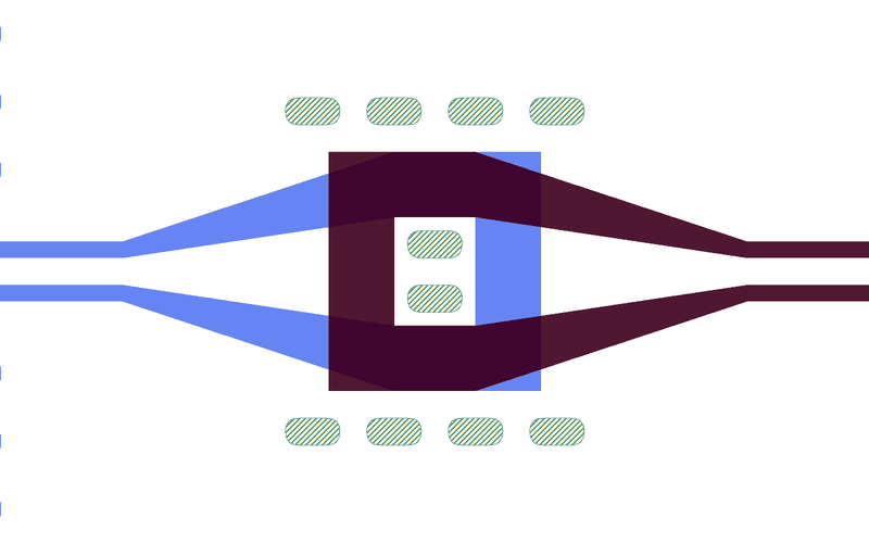
A TSV transition (TDN_IN_A) with both its lines: the feed line tapers into the front pad (1t1, blue), the two
signal vias carry it through the chip, and the back pad (1b1, dark red) tapers out the other way into the underpass.
Eight ground vias stitch the two ground planes. The PDK cheese band stays outside the transition’s keep-out box.
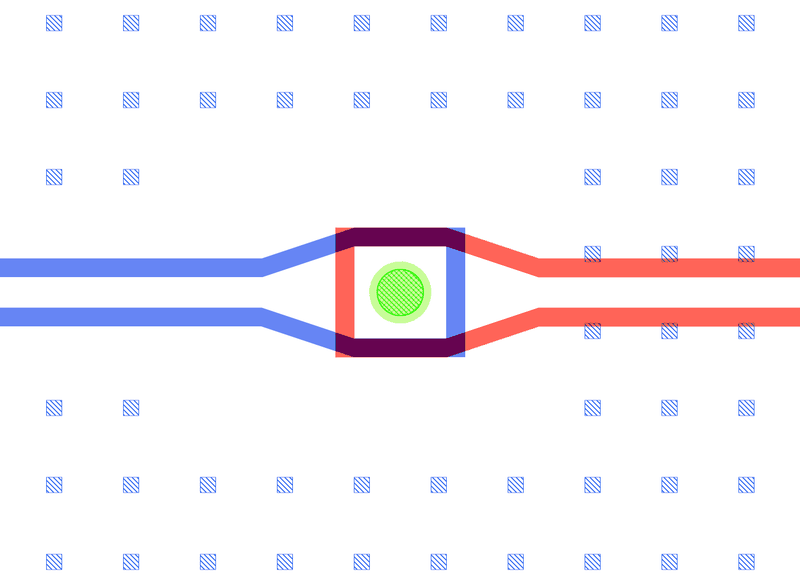
A bump transition (B_IN_A): QcFlipChipConnectorRf with QPDK’s 30 µm pads and 6 µm gap, the bottom-chip pad (blue),
the top-chip pad (red) and the 15 µm bump on its under-bump metal in the middle.
In the whole-chip picture some ground bumps seem to sit on the serpentines: 20 of the 609, in the rows at y 3500 and
6500 µm, fall on a serpentine’s legs, and the dark dots on those legs are where a bump’s marker is drawn over the line.
That is only the top-down view, which draws every face on one plane. The serpentines run on the top chip’s back (MB2,
2t1) and the bumps sit between the two front faces (1t1 and 2b1), so the whole top chip lies between them. Under
those 20 bumps the top chip’s front face is solid ground, so each one joins ground to ground like the rest. The only
bumps on a line are the four signal bumps of the bump transitions. QPDK’s own picture shows its bump arrays crossing
the serpentine legs in the same way.
The PDK fab layer map writes the two front faces: 1t1 to 1/0 and 3/0, 2b1 to 800/0, the vias of both chips to
700/0 and the bumps to 801/0 and 802/0. It has no fab layer for the backside faces, so export_fab leaves out the
1b1 and 2t1 etch (the underpasses, the serpentines, the backside pads and tapers) and their copies of the vias, and
says so with a FabLayersDropped warning. The design file keeps them. The cheese holes stay at least 13 µm from every
TSV and bump.
The notebook also exports one transition of each kind as a sim group, each for Q3D and for a driven (S-parameter)
run: TSV_IN_A on 1b1 and 1t1, BUMP_IN_A on 1t1 and 2b1, TSV_TOP_A on 1t1, 2b1 and 2t1. The exports pass the
library’s geometry check; none has been solved.
LOM estimates
There is nothing to estimate: the chip has no qubits or resonators. The netlist check shows two conductors, one per line, each between two 50 Ω launchers; every TSV and bump transition along the way is a pass-through section with no lumped L or C.
Build spec
The rest of this page is the spec the notebook was built from, with every component, route and position, and what the rebuild changed.
Source: qpdk/samples/tsv_flip_chip_test_chip.pic.yml
· cells qpdk/cells/tsv.py, bump.py, chip.py · licence MIT (“Copyright (c) 2024 gdsfactory”, checked in LICENSE)
· read on 2026-11-02.
Image: docs/_static/images/tsv_flip_chip_test_chip.png.
What it is: two mirrored through lines, a (north) and b (south). Each one leaves a launcher on M1 and drops through a
TSV pair to a backside (MB) underpass, then comes back up to M1. It crosses an indium-bump transition to the top chip (M2),
goes through a top-chip TSV to a serpentine on the top chip’s backside (MB2), then returns the same way to a second
launcher. Three 29 × 7 indium-bump arrays tie the two ground planes together. There are no resonators or qubits; this
chip tests the interconnect.
Frame: bottom chip edge 10000 × 10000 at (−5000, −5000), top chip 6000 × 6000 at (−3000, −3000) (both 100 µm etched
frames). Box (0, 0, 10000, 10000), Designer = source + (5000, 5000), top chip over (2000…8000)².
Faces: M1 = bottom-chip front (KQC 1t1), MB = bottom-chip back (1b1), M2 = top-chip front facing down (2b1),
MB2 = top-chip back (2t1); all four are in kqcircuits.defaults.default_faces. CPW 10/6 µm on every face (cpw,
cpw_backside, cpw_top, cpw_top_backside), bend radius 100 µm.
Components (line a at Designer y 6000; line b mirrored at y 4000)
instance |
catalog ref |
key params (units) |
at (x, y) Designer |
rot |
notes |
|---|---|---|---|---|---|
PIN_A / PIN_B |
|
QPDK launcher: pad 200 × 200, gap 110, taper 100 |
(510, 6000) / (510, 4000) |
270 (faces east) |
launcher_in (−4900, ±1000); port 410 µm in from the outer etch, which is 100 µm from the die edge |
POUT_A / POUT_B |
|
same |
(9490, 6000) / (9490, 4000) |
90 (faces west) |
launcher_out (4900, ±1000) rot 180 |
TDN_IN_x |
|
defaults (QPDK’s): tapers 100, pad 40 × 30, pad_gap 24, |
(900, y) |
0 |
M1 → MB |
TUP_IN_x |
|
same |
(1700, y) |
180 |
MB → M1 |
B_IN_x |
|
connector_a 30, connector_b 6, bump ⌀ 15, UBM ⌀ 20, no ground bumps |
(2250, y) |
0 |
M1 → M2 |
TT_IN_x |
|
same as TDN_IN |
(2800, y) |
0 |
M2 → MB2 |
TT_OUT_x |
same |
same |
(7200, y) |
180 |
MB2 → M2 |
B_OUT_x |
|
same as B_IN |
(7750, y) |
180 |
M2 → M1 |
TDN_OUT_x |
|
same |
(8300, y) |
0 |
M1 → MB |
TUP_OUT_x |
|
same |
(9100, y) |
180 |
MB → M1 |
BUMPS_C / _N / _S |
|
29 cols × 7 rows, pitch 200, ⌀ 15, UBM ⌀ 20 |
centres (5000, 5000), (5000, 7100), (5000, 2900) |
— |
each 5600 × 1200 µm |
A CpwTsvTransition has port a on its front face and b on the back face of the same chip; a
QcFlipChipConnectorRf has a on 1t1 and b on 2b1. At rotation 0, a faces west.
Routes (line a; b mirrors y about 5000)
route |
face |
from → to |
waypoints (Designer) |
|---|---|---|---|
FEED_IN |
M1 (1t1) |
PIN.a → TDN_IN.a |
straight |
UNDER_IN |
MB (1b1) |
TDN_IN.b → TUP_IN.b |
(1035, 6000), (1200, 6000), (1200, 6400), (1400, 6400), (1400, 6000), (1565, 6000) (b: 3600) |
BOT_IN |
M1 (1t1) |
TUP_IN.a → B_IN.a |
straight |
TOP_IN |
M2 (2b1) |
B_IN.b → TT_IN.a |
straight |
TOP_BACK |
MB2 (2t1) |
TT_IN.b → TT_OUT.b |
serpentine x 3200 → 6800 in 400 µm steps between y 6000 and 6600 (10 legs; b: 4000/3400) |
TOP_OUT |
M2 (2b1) |
TT_OUT.a → B_OUT.b |
straight |
BOT_OUT |
M1 (1t1) |
B_OUT.a → TDN_OUT.a |
straight |
UNDER_OUT |
MB (1b1) |
TDN_OUT.b → TUP_OUT.b |
(8435, 6000), (8600, 6000), (8600, 6400), (8800, 6400), (8800, 6000), (8965, 6000) |
FEED_OUT |
M1 (1t1) |
TUP_OUT.a → POUT.a |
straight |
No route names its face: each is drawn on the face of its start port. The first and last underpass waypoints, 20 µm from the ports, are not QPDK’s: the router leaves a port straight for one bend radius (100 µm) before the first corner, and QPDK’s first corner is only 185 µm from the port. A waypoint that close to a port on its axis counts as the port’s stub, so the centre line stays QPDK’s.
Launchers, pads, test structures, markers, labels
4 launchers, 609 ground bumps (3 × 203). The Quantcore die frame replaces the bottom chip’s 100 µm etched edge; the top chip’s edge is not drawn.
LOM node structure
Two independent 2-port through lines with four 50 Ω ports and no resonant elements. A full model would be a chain of CPW segments with lumped transitions (a TSV pair or a bump: series L plus pad C) in which the MB2 serpentine sets the delay. The netlist of the build has no lumped transitions: each line is one conductor between its two launchers.
Targets
None. The test checks continuity and return loss of every face transition.
Sim groups
group |
selection |
faces |
analyses |
|---|---|---|---|
TSV_IN_A |
TDN_IN_A, margin 60 µm (the cut stubs of FEED_IN_A and UNDER_IN_A) |
1b1, 1t1 |
|
BUMP_IN_A |
B_IN_A, margin 60 µm (BOT_IN_A, TOP_IN_A) |
1t1, 2b1 |
|
TSV_TOP_A |
TT_IN_A, margin 60 µm (TOP_IN_A, TOP_BACK_A) |
1t1, 2b1, 2t1 |
|
The 60 µm margin keeps each box edge on a straight of the lines it cuts: the export moves box edges off bends on 1t1 only. The driven jobs use the library’s default frequencies (adaptive mesh at 6 GHz, sweep 4 to 9 GHz).
Build
The notebook is examples/designs/qpdk/tsv_flip_chip_test_chip.ipynb. What the rebuild uses:
TSV transitions:
CpwTsvTransitionat its defaults, which are QPDK’stsv_transition_double_sided, withtsv_margin=2µm (QPDK’s via landing-pad margin) in place of KQC’s 30 µm ground-grid avoidance. Its 3/0 keep-out is the box around both pads, both tapers and every via.Bump transitions:
QcFlipChipConnectorRfinstances with QPDK’s pad, gap and bump. KQC’s cell tapers over the pad’s length (30 µm; QPDK 10 µm) and always draws an under-bump metal (⌀ 20 µm here; QPDK draws none).Faces: the transitions record the face of each port and the routes take theirs from the start port. The DRC checks each face on its own: no errors, no warnings and no PDK design warning.
Not supported yet, or not done here:
The LOM has no lumped L or C for a transition (via height, bump, width steps): it is a pass-through section.
PDK v3 has no fab layer for 1b1 or 2t1, so the backside metal is not in the mask (see above).
No multi-face simulation has been solved, and AEDT has not imported one yet; whether Q3D joins the face sheets and the via and bump pillars as KQC intends is not confirmed.
The DRC’s
outside_chipand frame rules use the bottom chip’s box on every face, so the top chip’s transitions and lines are not checked against the top chip’s outline.
Quantcore PDK rebuild
The notebook rebuilds the chip on the Quantcore PDK: the topology, positions and sizes are QPDK’s, the process is Quantcore’s.
Notebook: examples/designs/qpdk/tsv_flip_chip_test_chip.ipynb.
Chip: the Quantcore die frame (L dicing markers 1000/0, 3 × 3 alignment grids 1001/0, chip boundary 100/0, device ID QPDK-TSV) on the source’s 10 × 10 mm bottom chip; the top chip has no frame in the PDK and is not drawn.
Pads: the launchers’ outer etch is 100 µm from the die edge (
edge="auto"), where QPDK’s launchers already sit.Stack: sapphire 650 µm, εr 10.25 on both chips (the PDK default), with the PDK’s 8 µm chip gap in the sim groups.
Cheese: the source has none, so the PDK band (chip
cheese: "auto") around the front-face features, clear of the TSVs and bumps.Kept: both lines with QPDK’s transition, bump and waypoint positions, the TSV transitions’ tapers, pads, gaps and vias, the bump transitions’ pads and bump, the underpasses and serpentines, and the 609 ground bumps.