Flux-pumped SQUID JPA
A lumped JPA whose inductor is a DC SQUID. A static flux tunes the mode, and a pump on the flux line at twice the signal frequency modulates the SQUID (three-wave mixing). The layout follows twpa-sim’s squid_jpa family (MIT), which leaves the coupling and flux line external; the rebuild draws both.
This chip is a small flux-pumped amplifier: a coupling capacitor on the signal side, the SQUID with its shunt capacitor, and a flux line that arrives from a second pad.
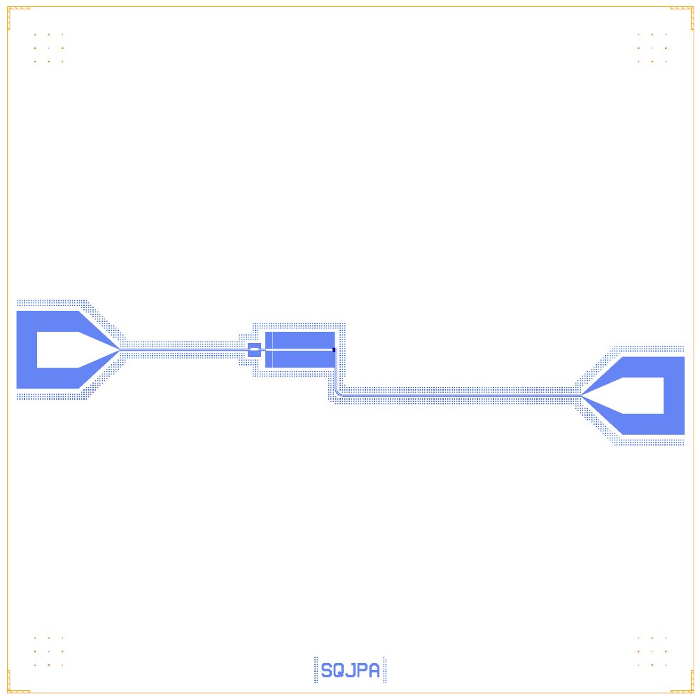
At a glance
Notebook |
|
Source |
twpa-sim |
Chip |
7.5 × 7.5 mm Quantcore die, sapphire 650 µm |
On the chip |
1 |
Builds today |
yes (layout built on 2026-11-19 in 5 s) |
How the notebook builds it
The amplifier notebooks use six Design segments (die, pads, feed, nonlinear element, routing, whole chip); see the notebook template.
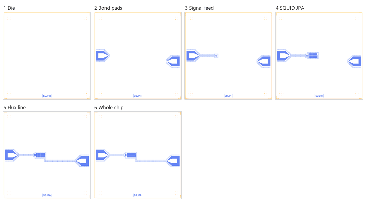
Die. The empty die with the QCT frame and the device ID
SQJPA.Bond pads. The signal pad on the west edge and the flux / pump pad on the east edge.
Signal feed. The coupling capacitor (14 fingers × 90 µm) and its 50 Ω line.
Nonlinear element. The SQUID JPA: the largest PDK SQUID, a shunt capacitor and the flux line.
Routing. The flux / pump line from the SQUID to the east pad.
Whole chip. The
jpasim group and the saved design.
LOM estimates
Numbers are from a run of this notebook on 2026-11-19 (Setup, Design, Check and the LOM cells, 7 s). This is an amplifier, so the LOM section gives gain and phase matching, not qubit frequencies. The JPA’s resonance is tuned by flux:
Φ (Φ0) |
f0 (GHz) |
κ/2π (MHz) |
Q_ext |
K/2π (MHz) |
|---|---|---|---|---|
0 |
6.946 |
42.0 |
166 |
9.34 |
0.1 |
6.774 |
40.0 |
170 |
9.34 |
0.2 |
6.247 |
34.2 |
183 |
9.33 |
0.3 |
5.324 |
25.0 |
213 |
9.33 |
0.4 |
3.860 |
13.3 |
291 |
9.32 |
At 0.3 Φ0 the tuning slope is df0/dΦ = -11.54 GHz/Φ0 with κ/2π = 25.0 MHz. Flux-pumped gain against the pump strength r:
r |
peak gain (dB) |
pump flux Φ_p (mΦ0) |
|---|---|---|
0.5 |
4.44 |
1.08 |
0.7 |
9.31 |
1.52 |
0.8 |
13.2 |
1.73 |
0.9 |
19.6 |
1.95 |
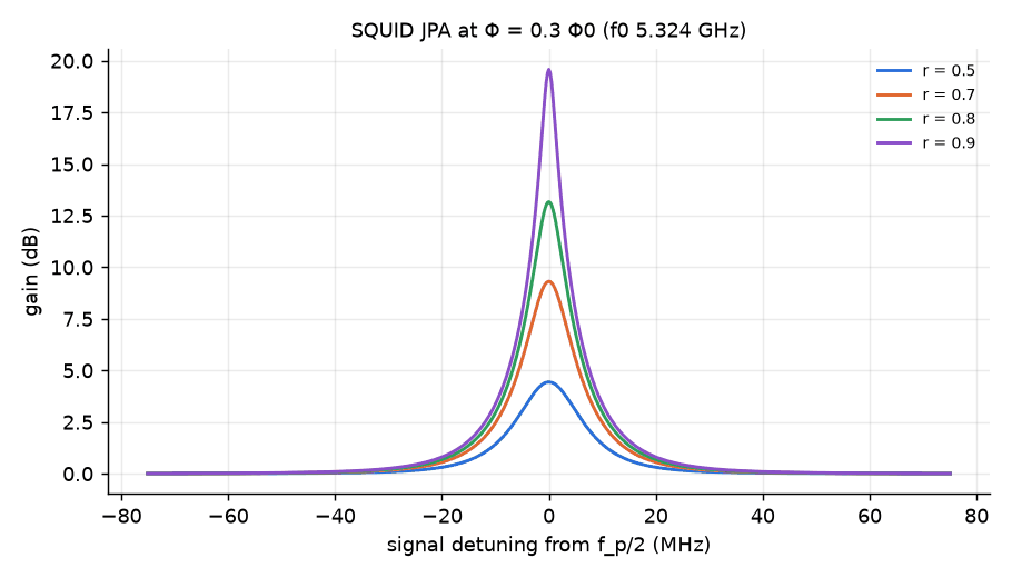
These are lumped-model estimates (component formulas and calibration), not FEM results. The LOM page says how far to trust them.
Build spec
The rest of this page is the detailed spec the notebook was built from, with every component, port, route and length.
Source · licence: mandalsoumyajit/twpa-sim (MIT): src/twpa/layout/generate.py (family squid_jpa), examples/layout/squid_jpa.json. Die: 7.5 × 7.5 mm PDK die, PDK frame, sapphire 650 µm, Nb trilayer junctions. Notebook and design: examples/designs/amplifiers/twpa_sim_squid_jpa.ipynb / .json.
Components
instance |
catalog ref |
key params |
notes |
|---|---|---|---|
P_SIG, P_FLUX |
|
west / east edge |
|
CC |
|
14 fingers × 90 µm |
|
JS |
|
Quantcore Squid (2 × 2.0 × 2.0 µm), flux line, 45 fingers/side × 180 µm IDC |
Routes
route |
from → to |
type |
|---|---|---|
L_SIG |
P_SIG.a → CC.a |
CPW |
L_FLUX |
JS.flux → P_FLUX.a |
CPW, one waypoint |
LOM node structure
island (C_shunt, SQUID to ground at the static bias flux_phi0), then C_c π, then pad; flux is a control
Targets (from the source)
none stated (illustrative: f0 ≈ 70 GHz)
Simplifications / PDK differences
PDK SQUID; planar IDC; coupling and flux line drawn (external in the source); junctions are flagged pdk_rn where present (amplifier junctions are far below the qubit R_n window).