Tutorial 1: Chip 12
examples/tutorials/01_chip12_coupled_chip.ipynb rebuilds a legacy nine-qubit test chip, “chip 12”, in the Quantcore
PDK, step by step, and runs the whole loop on it. The chip is an internal Quantum Metal design; its positions and
options are in examples/designs/legacy/_legacy_b.py and its spec is Chip 12.
The design notebook builds the same chip in one cell; this tutorial builds it in small steps. It is the first
tutorial where the layout comes from a source and the PDK rules change it.
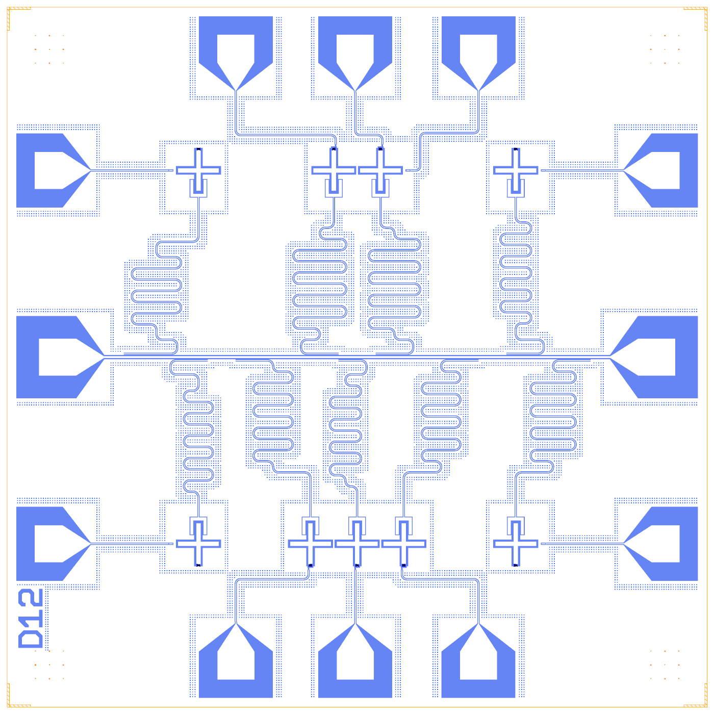
Section 6: all nine qubits, twelve launchpads, readouts and control lines, with device ID D12.
What the chip is
A 7.5 × 7.5 mm coupled-qubit test chip:
one 20/12 µm feedline across the die centre with nine λ/4 readouts, 4.3 to 6.3 mm long;
nine
TransmonCrossXmons (metal:wrapper);Q1-Q2, a direct pair: their arm tips face each other across a 20 µm ground strip;
Q5-Q8-Q6, a tunable-coupler triple: Q8 is a flux-tunable Xmon between Q5 and Q6, with its own readout;
five flux lines and five drive lines, each to its own launchpad (ten line pads and two feed pads).
The PDK wins wherever it has a rule, so the rebuild differs from the source:
From the source |
What the PDK changes |
|
|---|---|---|
Pads |
Legacy launchpad positions |
Outer etch edge 100 µm from the die edge |
Junctions |
External junction cells, no values |
Trilayer |
Cheese |
None |
The PDK band around the 3/0 keep-outs |
Readouts |
Lengths and couplers |
Couplers pinned with |
Values |
No qubit targets |
Out-of-margin values are flagged (DRC design warnings), never retuned |
The sections
Section |
What it does |
What comes out |
|---|---|---|
1 PDK facts |
The PDK rules this chip uses |
A table of the rules and what each is used for |
2 Die and frame |
|
The empty die with its frame |
3 Pads |
Two feed launchpads and ten line pads, |
A table: every pad’s outer etch edge is 100.0 µm from the die edge |
4 Feedline |
|
A 5380 µm feedline; it runs right to left, so its “right” side is the top half of the chip, which decides the hanger |
5 Components |
Nine Xmons with junctions; |
Junction L_J 6.7344 nH, C_J 15 fF; arm-to-arm estimate C_arm = 1.67 fF |
6 Routes |
Nine λ/4 readouts through |
A table of drawn against legacy lengths (all equal, R0 5493 µm to R8 4300 µm) and the full chip picture |
7 DRC |
Errors, warnings and PDK design warnings |
0 errors, 30 warnings (all |
8 Netlist and LOM |
|
24 nodes, 74 branches; a small netlist of Q1, Q2, R1, R2 |
9 LOM simulation |
Each qubit with its readout, the pair, the triple |
Tables of f_q, α, f_r, κ, χ; J and ZZ of Q1-Q2; three hybridised modes of Q5-Q8-Q6 |
10 FEM stage 1 |
Sim groups and the subset check |
Convergence, C-matrices, eigenmodes, FEM-filled capacitances |
11 FEM stage 2 |
The subset values in the whole netlist, then feedback |
LOM versus FEM, J on FEM values, a revision with new readout lengths |
12 Iterate |
Claw 150 to 180 µm on a copy of the design |
A before/after table, design hash and DRC |
13 Build and export |
|
Fab layer table |
14 Snapshots |
The pair, a SQUID, a readout short, the fab view, the legacy screenshot |
Pictures |
15 Summary |
Matches and differences against the source |
A table |
3 to 6: pads, feedline, qubits, routes
Twelve pads are added in one with d.batch(): block, so the design is rebuilt once instead of twelve times. Every pad
is asked at its legacy position and slid to the 100 µm rule. The feed pads are 400 × 400 µm (20/12 µm trace); the ten
line pads are 400 × 300 µm (10/6 µm trace).
The Xmons have a 220 × 50 µm cross in a 20 µm gap and a 150 µm readout claw (6 µm gap). Q1-Q2, Q5-Q8 and Q8-Q6 couple
through their facing arm tips; no route joins them, so d.couple(...) declares each with a coupled-strip estimate of
1.67 fF. The Q1_Q2 FEM group gives the real value.
Readout lengths came out equal to the legacy ones. The flux and drive lines run through the legacy corner points as waypoints; the pads moved to the edge, so the first straight of each line is longer.
7 to 9: DRC, netlist and the LOM
The legacy readout lengths were drawn for a bare λ/4 (no claw), so each legacy length’s bare frequency is the readout target. Each qubit with its readout, the feedline acting as a load:
Qubit |
f_q (GHz) |
α (MHz) |
Readout f_r, LOM (target) GHz |
|---|---|---|---|
Q0 |
5.0591 |
-196.9 |
4.9357 (5.7361) |
Q1 |
5.0411 |
-146 |
4.4242 (5.0317) |
Q2 |
5.0401 |
-145.2 |
4.5015 (5.1317) |
Q3 |
5.0325 |
-146 |
5.7585 (6.7936) |
Q4 |
5.0331 |
-146.4 |
5.937 (7.041) |
Q5 |
5.0248 |
-135.7 |
5.226 (6.0594) |
Q6 |
5.0277 |
-139.6 |
5.283 (6.1396) |
Q7 |
5.046 |
-124.6 |
4.8085 (5.5375) |
Q8 |
5.0352 |
-146.8 |
6.1513 (7.3276) |
Every Xmon lands near 5.0 GHz (inside the PDK band) with α about -145 MHz. The claw adds about 125 fF at each readout’s open end, so the loaded readouts sit 0.6 to 1.2 GHz below their bare λ/4. Q0 and R0 come out nearly degenerate and hybridise (χ = 64.7 MHz), and Q7 and R7 are close (χ = -22.7 MHz). The notebook does not retune them: that is a design decision.
The direct pair Q1-Q2, with the same junction on both, shows two hybridised modes at 5.1220 and 5.1828 GHz and J = 29.5 MHz. That J comes from the rough 1.7 fF arm estimate. With Q2 detuned (L_J 7.4 nH) the static ZZ is -1.12e+04 kHz, in the MHz range: the reason Q8 sits between Q5 and Q6 as a tunable coupler. The triple at zero flux (all three resonant) gives three hybridised modes at 5.0932, 5.1529 and 5.1836 GHz.
10 and 11: the FEM stages
The sim groups cut the chip into jobs a workstation can solve:
Group |
Analysis |
Box |
Gives |
|---|---|---|---|
|
|
The qubit and 300 µm; the readout is cut at the claw |
C_island, C_g, C_claw |
|
|
Q1 and 150 µm; the readout and flux lines leave the box as 50 Ω lines |
The qubit’s own mode: f_q, α, p_J |
|
|
Q1, its whole readout and 100 µm, with the feedline cut at both ends |
f_q, f_r, χ, κ |
|
|
Both qubits and 300 µm |
The arm-to-arm capacitance, hence J |
|
|
The triple and 300 µm |
The tunable-coupler capacitances |
The eigenmode job of the whole Q1_R1 box (a 1.3 × 2.9 mm box) did not finish within 20 minutes on the workstation,
which is why the notebook splits it into Q1_q and Q1_R1e.
The kept results (fast settings):
Job |
Passes |
Last Δ / target |
Converged |
Wall time |
|---|---|---|---|---|
|
8 |
1.24 / 2.0 % |
no |
60.6 s |
|
8 |
1.33 / 2.0 % |
no |
41.1 s |
|
3 |
0.591 / 1.0 % |
yes |
123.6 s |
|
3 |
1.67 / 1.0 % |
no |
276.8 s |
The Q1_R1 C-matrix gives C_g 10.883 fF against the 5.2 fF estimate and C_claw 111.388 fF. The eigenmode of Q1 alone
gives a dressed f_q of 4.7564 GHz and α of -126.9 MHz (p_J 0.9876). Q1_R1e gives f_q 4.7212 GHz and a cross-Kerr
χ of -26.451 MHz.
Stage 2 fills the branches the Q3D jobs simulated (9 branches) into the whole netlist; 40 branches keep their
estimates. The LOM then runs pair by pair, because QuCat on all nine qubits at once is far too slow. For Q1 and Q2
the LOM on the subset Q3D moves f_q by +1.6 % and +3.1 %, and the readout χ from -1.644 to -9.158 MHz (Q1) and from
-2.369 to -10.86 MHz (Q2). Against pyEPR on Q1_q the filled LOM f_q is 7.2 % high (5.123 against 4.756 GHz). For
the pair, the FEM arm-to-arm capacitance is 1.153 fF (against 1.67 fF) and J drops from 29.53 to 21.91 MHz.
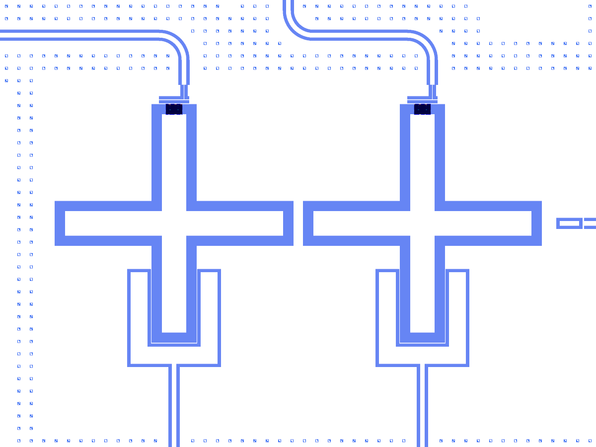
Section 14: the direct-coupled pair Q1-Q2 with their readouts and control lines.
Feedback moves each readout’s length: the λ/4 scales with f / target. For example R0 goes from 5493 to 4727 µm and R8
from 4300 to 3610 µm. The result is a revision examples/tutorials/designs/t01_chip12_fb.json (DRC clean), exported
to a fab file. The consensus on the whole netlist reports 0 of 9 targets within tolerance: the revision is the first step, and
the loop closes by running stage 2 on it.
12: iterate
Lengthening Q1’s claw from 150 to 180 µm on a copy of the design (Designer.load):
Quantity |
Before |
After |
Change |
|---|---|---|---|
Q1 f_q (GHz) |
5.0411 |
5.0264 |
-0.3 % |
Q1 α (MHz) |
-146.02 |
-144.81 |
+0.8 % |
R1 f_r (GHz) |
4.4242 |
4.3754 |
-1.1 % |
R1 χ (MHz) |
-1.6439 |
-1.883 |
-14.5 % |
R1 κ (MHz) |
0.15343 |
0.14668 |
-4.4 % |
The design hash changes from b08ee7bf... to 818a245f... and the DRC stays clean. One parameter moved; the layout,
DRC, netlist and LOM followed.
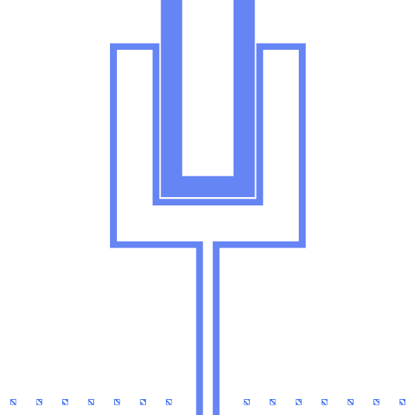
Before: Q1’s readout claw at 150 µm.
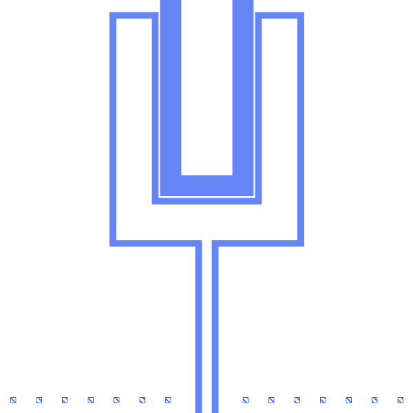
After: the claw at 180 µm.
13: export
export_fab keeps the build’s cheese (14723 holes) and rounds corners. With cheese=False, rounding=False it writes
0 holes and 42 M1 polygons. The CLI equivalents are in the notebook:
qcc build examples/tutorials/designs/t01_chip12.json --show, qcc design drc ..., qcc circuit export ...,
qcc circuit simulate ....
Pitfalls
Hangers by arclength (
s=) slide when a pad moves; usenear=as the notebook does.squid_aandsquid_bare junction attachment points, not route ends. They show asdangling_portwarnings. That is expected.A SQUID gets the same total L_J as a single junction, so each of its two junctions has twice the R_n. The PDK window judges the device’s parallel R_n.
At a 200 µm claw the claw would reach the cross’s side arms, and the DRC flags it as
pdk_claw. The notebook stops at 180 µm.The FEM results of sections 10 and 11 belong to the original geometry. After section 12 changes the design hash they are stale: re-run them to refresh.
The Q3D jobs are fast-setting results, not converged (Δ 1.2 to 1.3 % against 2 %).
FEM_WHOLE = Truealso solves the whole chip as one Q3D (chip_q3d_cmatrixis kept). Whole-chip eigenmode or driven runs take hours and over 30 GB.
Tutorial 2 uses a chip with no public layout, built from device data.