Xmon capacitance (SQDMetal)
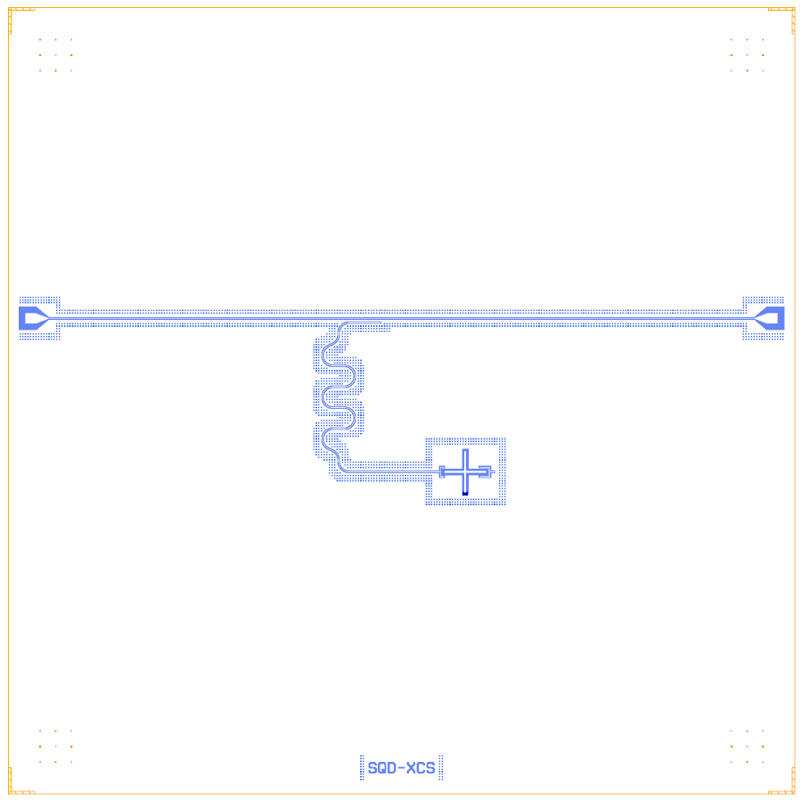
One cross transmon (Xmon) whose readout meander ends in an open end 40 µm below a through line, so it couples along an open-ended section. It is SQDMetal’s Palace capacitance example (Apache-2.0), rebuilt on the Quantcore PDK with the metal:TransmonCross wrapper.
Build this one to learn an open-ended coupled readout and a second, unused claw (the bus claw stays open).
At a glance
Notebook |
|
Source |
SQDMetal example |
Chip |
7.5 × 7.5 mm Quantcore die, the source’s 4.6 × 2.4 mm area in its middle, CPW 10 / 6 µm |
On the chip |
2 launchpads · 1 transmission line · 1 cross transmon · 1 meander readout with an open end |
Builds today |
yes (layout built on 2026-11-19 in 10 s) |
How the notebook builds it
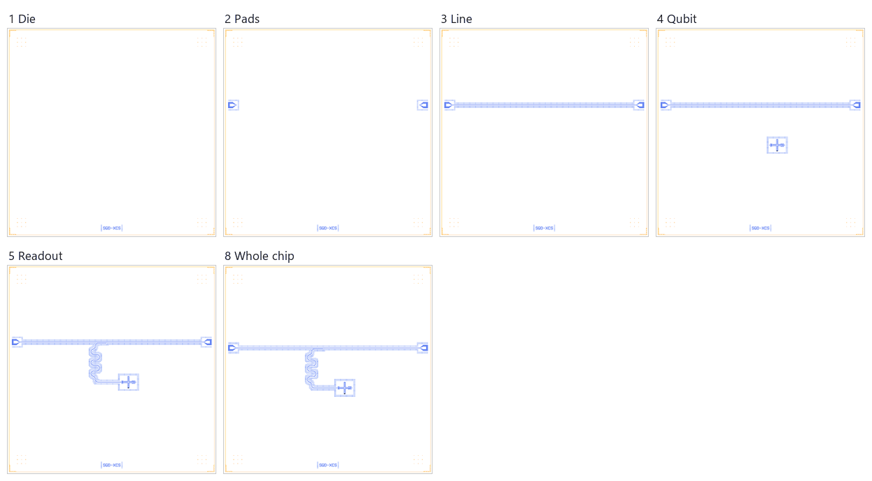
Die. The Quantcore die with the frame and the device ID.
Bond pads. Two launchpads on the 100 µm pad rule.
Line. The through line between the pads (2.7 mm longer than the source’s).
Qubit. One
metal:TransmonCrosswith the source’s connection pads.Readout. A meander up to an open hanger end 40 µm below the line.
Coupling. None: the bus claw stays open.
Control lines. None.
Whole chip. One sim group, centring, save.
LOM estimates
Numbers are from a run of this notebook on 2026-11-19 (Setup, Design, Check and the LOM cells, 9 s): QuCat normal modes with QuTiP dressed values.
mode |
kind |
f (GHz) |
κ (MHz) |
A (MHz) |
participation |
|---|---|---|---|---|---|
Q1 |
qubit |
5.977 |
0 |
184 |
J_Q1 1.00 |
R1 |
resonator |
16.11 |
0.0247 |
0 |
R1 1.00 |
parameter |
LOM (QuTiP) |
target |
|---|---|---|
|
5.79 |
– |
|
-199 |
– |
|
-0.137 |
– |
|
16.1 |
– |
|
0.0247 |
– |
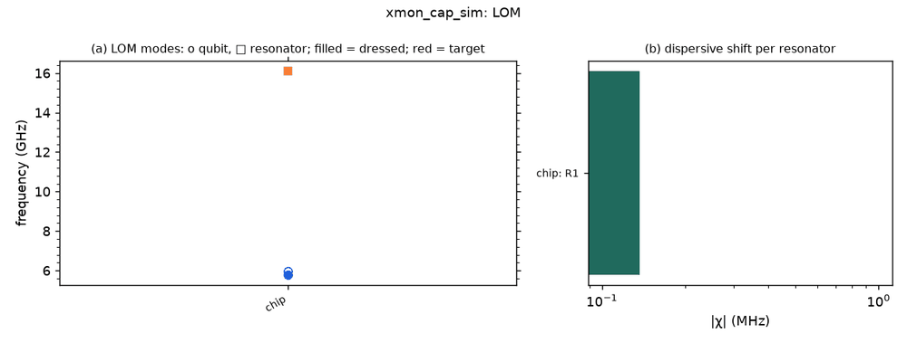
These are lumped-model estimates from component formulas and calibration, not FEM results. The LOM page says how far to trust them.
Build spec
The rest of this page is the detailed spec the notebook was built from: every component, port, route and length.
Source: doc-sphinx/source/examples/Palace_Capacitance_Xmon_Gmsh.ipynb
· licence Apache-2.0 (verified) · read on 2026-11-02. There are no stored outputs. Pure Quantum Metal parts
(TransmonCross, RouteMeander, RoutePathfinder, LaunchpadWirebond, OpenToGround), meshed with Gmsh for a
Palace capacitance run on silicon.
What it is: one grounded cross transmon with two claws (readout east, bus west). The readout claw runs a 3.7 mm meander
to an open end placed 40 µm below a through transmission line. The open-end lead (300 µm start_straight) runs
parallel to the line, so the coupling is an open-ended coupled section. Two small launch pads.
Frame: chip 4.6 × 2.4 mm centred at (0, −1) mm, substrate 280 µm. Box (0, 0, 4600, 2400),
Designer = source + (2300, 2200). CPW 10/6 µm.
A first build uses Xmon, BondPad and a hanger with end="open".
Components
instance |
catalog ref |
key params (units) |
at (x, y) Designer |
rot |
notes |
|---|---|---|---|---|---|
LP1 |
|
(300, 2200) |
270 (faces E) |
Metal orientation 360 at (−2, 0) mm |
|
LP2 |
|
(4300, 2200) |
90 (faces W) |
orientation 180 at (2, 0) mm |
|
Q1 |
|
claws [“e”, “w”]: |
(2907.5, 736) |
0 |
source (0.6075, −1.464) mm. |
Junction: not set in the notebook (capacitance only). For eigenmode use, assume junction={"Lj_nH": 12, "Cj_fF": 2}.
Routes
route |
from → to |
type, length |
hanger / waypoints |
notes |
|---|---|---|---|---|
TL |
LP1.a → LP2.a |
cpw 10/6 ( |
straight y 2200 |
|
R1 |
Q1.claw_e → TL.hanger |
meander 3700 (fillet 99.9) |
coupler centre x ≈ 1950 (source −350), length 300, side right (below TL travelling +x), ground_gap 18 (centre spacing 40 = 5 + 6 + 18 + 6 + 5), direction forward, end=”open” |
the open is |
s for R1 = 1950 − x(LP1.a). The bus claw (W) is left unconnected in the source.
Launchers, pads, test structures, markers, labels
2 launch pads. No fill, markers or labels.
LOM node structure
Q1: grounded cross island with Lj (assumed) to ground and two claw nodes (readout, bus) with C_g. R1 is open at both ends (claw at one, open-to-ground at the other), so it is a λ/2-type line of 3.7 mm (≈16 GHz on Si; the source runs capacitance only, not frequency). R1 couples to TL by coupled-line C/κ at its open end. TL: two 50 Ω ports.
Targets
None (capacitance-matrix extraction example).
Simplifications for a first rebuild
Use a
meanderwithend="open". If a λ/4 readout is wanted instead, keep the same layout withend="short"(≈ 8 GHz on Si) and say so in the design notes.Drop the bus claw if
Xmonclaw lists need ports to be used. Otherwise leaveclaw_wfree for a later bus.
Build
The notebook uses metal:TransmonCross (Metal: connector_location 0 = west arm, so the readout claw is on the west) and metal:LaunchpadWirebond; open hanger 400 µm from its corner (300 µm straight + 99.9 µm fillet), open end at the OpenToGround x.
Quantcore PDK rebuild
The notebook is a Quantcore PDK rebuild of the source, not a replica: the netlist, LOM and imported components are kept, and the process is Quantcore’s.
Notebook: examples/designs/sqdmetal/xmon_cap_sim.ipynb.
Chip: the Quantcore die frame (L dicing markers 1000/0, 3 × 3 alignment grids 1001/0, chip boundary 100/0, device ID where an edge is free; any brand text is QCT), on the 7.5 × 7.5 mm Quantcore die; the source’s 4.6 × 2.4 mm chip area is centred in it (
box=(-1450, -2550, 6050, 4950)), so every coordinate stays the source’s.Stack: sapphire 650 µm, εr 10.25 (the PDK default stack, used by the LOM estimates and every FEM export); the SQDMetal examples are on silicon (280–500 µm), so frequencies differ from the source’s.
Junctions: Quantcore Nb/AlOx/Nb trilayer junctions (
junction_typefromlayouts.registry.trilayer_junction): fingers on 2/0 + 4/0, spacer 50/0 with the 51–53/0 gradient, sized on the PDK junction rule (Nb Δ = 1.4 meV, I_c·R_n = πΔ/2e, R_n·A 13.5 kΩ·µm² and C_J 50 fF/µm² assumed); theTransmonCrossgets the PDK nominal junction, 0.5 × 0.6 µm fingers → R_n = 45 kΩ, L_J = 6.73 nH, C_J = 15 fF (in the 40–50 kΩ window) (the source sets no junction, being a capacitance-only run). Expected f_q ≈ 5.8 GHz (an estimate).Kept: the topology and the Metal components with the source’s options and positions, the 3.7 mm readout with its 300 µm coupled section and 40 µm spacing, the sim group.