KI spirals and a TWPA line
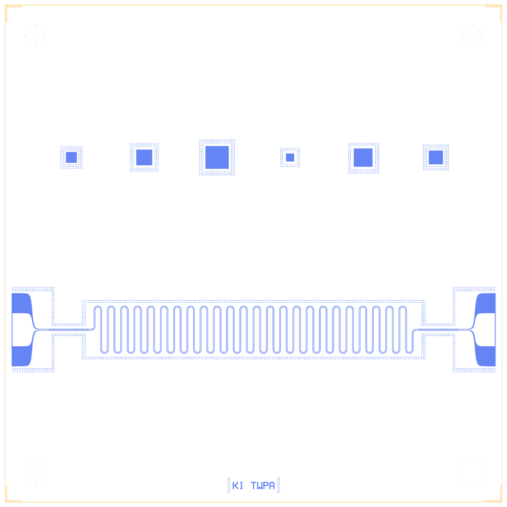
A structure sheet for kinetic-inductance (KI) devices, not a measured chip. A travelling-wave parametric amplifier (TWPA) style line runs from one bond pad to the other: a finger-loaded section, a meandered section and a second finger-loaded section, all 10/6 µm CPW. The fingers (2 µm wide, reaching into both grounds) add shunt capacitance per unit length, as a KI TWPA’s artificial line does. Above it sit six spiral inductors (double-Fermat and Fermat spirals), the compact high-inductance elements KI circuits use.
No KI or TWPA chip script exists in Quantcore’s library. The cells here are ported building blocks from the legacy files spiral.lym, draw.py and cpwe.py (internal; the finger line is from G. Long, Glasgow 2021), laid out as a sheet on the PDK die with the device ID KI TWPA. Build it to see the spiral and finger-line components side by side and how a snapped chain of CPW cells forms one continuous line.
At a glance
Notebook |
|
Source |
Legacy building blocks |
Chip |
7.5 × 7.5 mm Quantcore die, sapphire, CPW 10 / 6 µm |
On the chip |
2 |
Builds today |
yes, rebuilt from its JSON on 2026-11-19 in 2.2 s (the notebook itself was not re-run) |
Pictures
The sheet: the TWPA-style line at the bottom, six spiral inductors in their square pockets above.

The centre of spiral S3, a double-Fermat inductor: the metal line (white, 3 µm wide) winds out of the middle (an 80 µm view).
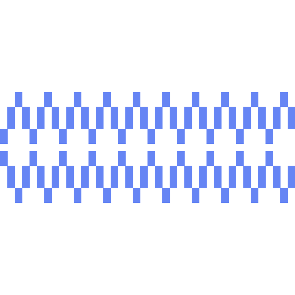
The finger-loaded line: 2 µm fingers reach into the grounds on both sides of the centre line (an 80 µm view).
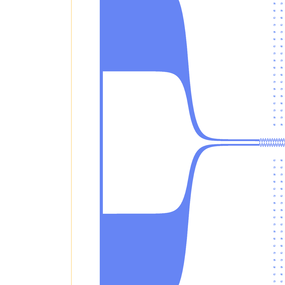
The left bond pad, an exponential taper into the 10 / 6 µm line.
LOM estimates
The notebook has no saved LOM output. The chip has no qubit and no resonator whose frequency the LOM estimates (it is a structure sheet).
Build spec
The rest of this page is the detailed spec the notebook was built from: every component, the changes made while rebuilding, and the notes.
Request: “import the kinetic-inductance and TWPA design chips to render, especially the
spirals”. Notebook: examples/designs/legacy/ki_twpa_structures.ipynb (+ .json).
Quantcore internal.
What the library holds
No KI or TWPA chip script exists in components/ (or the sibling project folders): no chip_* script, notebook
or GDS uses spirals, KI lines or a TWPA. The building blocks:
legacy source |
draws |
Quantcore cell |
|---|---|---|
|
Archimedean spiral path |
|
|
spiral by angle: 0 Archimedean, 1 Fermat, 2 double Fermat in/out (the double-Fermat branch has a typo, |
|
|
CPW with interdigital fingers into both grounds: the shunt-C-loaded artificial line of a KI TWPA |
|
|
meandered CPW, bond pad, taper, open end |
|
|
microstrip versions |
not ported (microstrip is ignored) |
The chip (Designer frame, 7.5 × 7.5 mm PDK die, ID KI TWPA)
instance |
cell |
params |
at |
|---|---|---|---|
PL |
|
pad 500 / gap 300, end 10, pad 50, taper 500 (exponential, weight 25), CPW 10/6 |
(250, 2600) |
F1, F2 |
|
150 fingers, 2 µm wide, 10 µm long, 2 µm apart, CPW 10/6 |
snapped: PL.a → F1, M1.b → F2 |
M1 |
|
r 50, straight 600, bias 0.5, 18 periods, CPW 10/6 |
snapped to F1.b |
PR |
|
as PL |
snapped to F2.b |
S1–S4 |
|
legacy sizes kept where they map ( |
(1000 + 1100 k, see notebook) |
PS1–PS4 |
|
square pocket 2 r_out + 40 µm |
same centres |
LOM
The line: one conductor PL → PR (50 Ω ports), finger sections with their shunt C (CpweFingerLine model). Spirals:
shapes without ports; the notebook tabulates N turns, wire length, geometric L (modified Wheeler, circular) and
kinetic L_k = L_□ ℓ / w for example sheet inductances (0.1 / 10 / 50 pH/□; the KI film is not in the PDK, so these are assumed
values). No sim groups.
Open
The actual KI / TWPA chip sources (if they exist elsewhere): add them to
components/to rebuild them as chips.Done: the
draw.spiralFermat / double-Fermat spirals are ported asSpiralLine, which the notebook uses.The KI film (material, thickness, sheet kinetic inductance) for the PDK.