Four-qubit ring (tutorial 1.3)
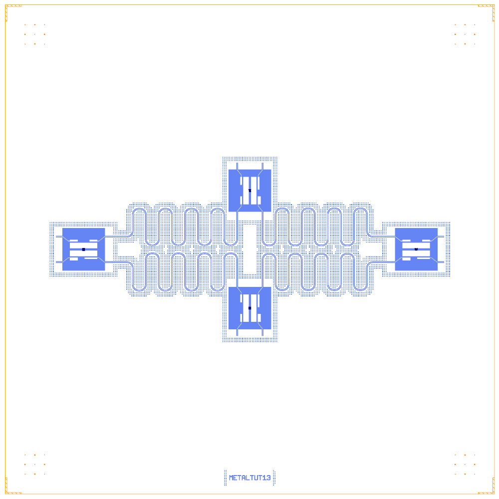
Four pocket transmons in a ring, joined by four meandered λ/2 buses. It has no readout, no launchpad and no control line. It is the core that Metal tutorial 2.21 and example 51 extend into a full chip. It is the Qiskit Metal tutorial 1.3 (Apache-2.0, © IBM and contributors). The Quantcore rebuild is distributed under GPL-3.0.
Build this one first if you want the smallest ring of coupled qubits. It shows how fixed-length bus meanders are routed between connection pads and how the PDK frames a chip that has no pads.
At a glance
Notebook |
|
Source |
Qiskit Metal |
Chip |
7.5 × 7.5 mm Quantcore die; the ring (about 6 × 2.7 mm) is centred in it |
On the chip |
4 pocket transmons · 4 λ/2 buses (6.0 and 6.1 mm) |
Builds today |
yes (layout built on 2026-11-19 in 8 s) |
How the notebook builds it
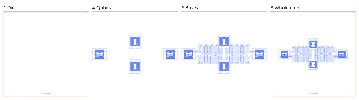
Die. The 7.5 mm die with the QCT frame (dicing marks, alignment grids, chip boundary, device ID).
Bond pads. None: the tutorial has no launchpads.
Readout line. None.
Qubits. Four Metal pocket transmons with Quantcore junctions, each with four connection pads.
Readout resonators. None: the outward pads stay open.
Coupling. Four fixed-length λ/2 buses close the ring between neighbouring qubits.
Control lines. None.
Whole chip. Sim groups for the FEM jobs (the whole ring, and qubit Q1 alone), the content centred in the die, the design saved.
LOM estimates
Numbers are from a run of this notebook on 2026-11-19 (Setup, Design, Check and the LOM cells, 16 s): QuCat normal modes with QuTiP dressed values.
group |
pair |
ZZ (kHz) |
neighbours |
hybridised |
|---|---|---|---|---|
Q1+cpw1+Q2 |
Q1-Q2 |
438 |
yes |
no |
Q3+cpw2+Q2 |
Q2-Q3 |
545 |
yes |
no |
Q3+cpw3+Q4 |
Q3-Q4 |
– |
yes |
yes |
Q1+cpw4+Q4 |
Q1-Q4 |
275 |
yes |
no |
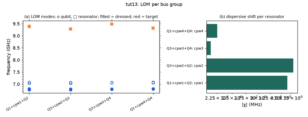
These are lumped-model estimates from component formulas and calibration, not FEM results. The LOM page says how far to trust them.
Build spec
The rest of this page is the detailed spec the notebook was built from: every component, port, route and length.
The
metal:references in this spec build as written, through themetal:wrapper (ports are the Metal pin names, parameters the Metal options). The Quantcore and KQC substitutions are optional.
Source: Quantum Metal docs/tut/1-Overview/1.3-Build-a-4-qubit-chip.ipynb. Licence Apache-2.0.
The chip has four TransmonPocket qubits, each with four connection pads (a/b/c/d), coupled in a ring by four
meandered CPW buses. There is no readout, no launchpads and no control lines; it is the core that 2.21 / 51 extend
into a full chip. The same core (with 3 pads per qubit) is used by tutorials 3.1–3.3, 4.01, 4.21 and
quick-topics/Managing-pins.
Chip: DesignPlanar default 9000 × 6000 µm, centred, so Designer = Metal + (4500, 3000). CPW 10/6 µm, fillet 90 µm.
Junctions are FakeJunction_01.
Later cells demonstrate design variables: cpw_width 25 µm, cpw_gap 12 µm, pad_width 450 µm, and bus
end_straight 100 µm. Build the 10/6 state; the variables cell is an optional variant.
A first build uses this substitution: Xmon with 2 claws for TransmonPocket.
Components
Metal TransmonPocket options: pad_width 425, pocket_height 650. Pads: a (+1, +1); b (−1, +1, pad_height 30); c (+1, −1, pad_width 200); d (−1, −1, pad_height 50). Only two pads per qubit are used.
instance |
catalog ref |
at (x, y) |
rot |
claw mapping (Metal pin used, Designer frame) |
|---|---|---|---|---|
Q1 |
|
(7050, 3000) |
270 (Metal 0) |
claw_w→N = b (6625, 3195) → Q4; claw_e→S = d (6625, 2805) → Q2 |
Q2 |
|
(4500, 2100) |
180 (Metal 90) |
claw_w→E = c (4695, 2525) → Q1; claw_e→W = a (4305, 2525) → Q3 |
Q3 |
|
(1950, 3000) |
90 (Metal 0) |
claw_e→N = a (2375, 3195) → Q4; claw_w→S = c (2375, 2805) → Q2 |
Q4 |
|
(4500, 3900) |
0 (Metal 90) |
claw_e→E = d (4695, 3475) → Q1; claw_w→W = b (4305, 3475) → Q3 |
Q1 and Q3 are both at Metal orientation 0. Q2 and Q4 are both at 90, so their pads point N/S. In Metal, Q2’s used pads point north and Q4’s point south, toward the centre.
Routes
route |
from → to |
type, length |
waypoints |
notes |
|---|---|---|---|---|
cpw1 |
Q1.claw_e → Q2.claw_w |
meander 6000 |
auto |
Metal Q1.d → Q2.c; lead_start 130, end_straight 100, asym +150 |
cpw2 |
Q3.claw_w → Q2.claw_e |
meander 6100 |
auto |
Metal Q3.c → Q2.a; asym −150, lead flipped |
cpw3 |
Q3.claw_e → Q4.claw_w |
meander 6000 |
auto |
Metal Q3.a → Q4.b; asym +150 |
cpw4 |
Q1.claw_w → Q4.claw_e |
meander 6100 |
auto |
Metal Q1.b → Q4.d; asym −150, flipped |
Launchers, pads, test structures, markers, labels
None in the source. For a testable chip, add the readout and charge pads of 51_four_qubit_chip.
LOM node structure
4 transmon islands (JJ to ground). 4 λ/2 buses forming a ring, B(Q1–Q2) 6.0 mm, B(Q3–Q2) 6.1 mm, B(Q3–Q4) 6.0 mm, B(Q1–Q4) 6.1 mm, each with C_g at both claws. There are no ports. The alternating 6.0/6.1 mm lengths detune neighbouring buses.
Targets (if stated)
None. Junction values are Metal defaults (Lj 10 nH, Cj 0); use junction={"Lj_nH": 10, "Cj_fF": 2}. A 6 mm λ/2 sits
near 10.5 GHz on sapphire (9.8 on Si), estimated.
Simplifications for a first rebuild
Use Xmon with 2 claws, rotated so the claws face the two ring neighbours; the claw_n stub is not needed.
Ignore asymmetry and flip; the meanders auto-place. This is the smallest multi-qubit Designer test (no pads), so check
d.lom()for 4 qubits + 4 buses.
Quantcore PDK rebuild
The notebook is a Quantcore PDK rebuild of the source, not a replica: the netlist, LOM and imported components are kept, and the process is Quantcore’s.
Notebook: examples/designs/metal/tut13_four_qubit_ring.ipynb.
Chip: the Quantcore die frame (L dicing markers 1000/0, 3 × 3 alignment grids 1001/0, chip boundary 100/0, device ID where an edge is free; any brand text is QCT), on the 7.5 × 7.5 mm Quantcore die: the ring (≈ 6 × 2.7 mm) fits, so the die is centred on Metal’s 9 × 6 mm chip centre (
box=(750, -750, 8250, 6750)) and every coordinate stays the source’s.Stack: sapphire 650 µm, εr 10.25 (the PDK default stack, used by the LOM estimates and every FEM export); Metal’s
DesignPlanardefault is silicon (εr 11.45, 750 µm), so the LOM capacitances, resonator frequencies and FEM jobs here are for sapphire rather than the source’s substrate.Junctions: Quantcore Nb/AlOx/Nb trilayer junctions (
junction_typefromlayouts.registry.trilayer_junction): fingers on 2/0 + 4/0, spacer 50/0 with the 51–53/0 gradient, sized on the PDK junction rule (Nb Δ = 1.4 meV, I_c·R_n = πΔ/2e, R_n·A 13.5 kΩ·µm² and C_J 50 fF/µm² assumed); all four qubits get the PDK nominal junction, 0.5 × 0.6 µm fingers → R_n = 45 kΩ, L_J = 6.73 nH, C_J = 15 fF (in the 40–50 kΩ window) (the source’sFakeJunction_01has no value). Expected f_q ≈ 7.1 GHz (an estimate), ≈ 2.4 GHz below the λ/2 buses. The pads still differ (padb30 µm,d50 µm high,c200 µm wide).Kept: the topology and every Metal component with the source’s options (through the
metal:wrapper), positions and orientations, every route’s end pins and total length, the sim groups (Metal’s own meander corner points, so the bus lengths are Metal’s).