Two feedlines, twelve resonators (design 14)¶
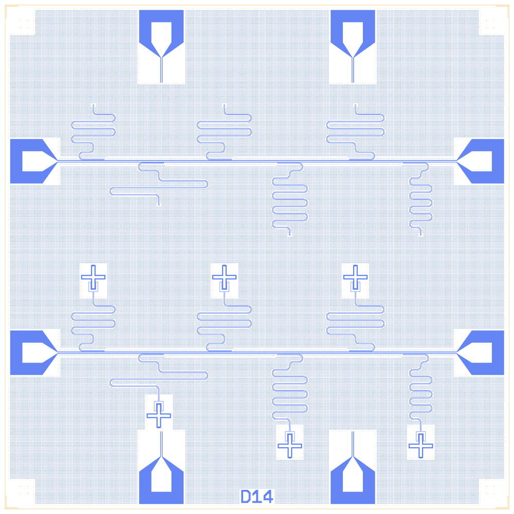
A 10 × 10 mm resonator chip with two straight 20/12 µm feedlines, one in the upper half and one in the lower half. Each feedline carries six λ/4 resonators, alternating above and below the line, at 6.5, 6.0, 5.5, 5.0, 5.25 and 7.0 GHz from left to right. On the lower feedline the open end of each resonator is the claw of an Xmon qubit; the upper feedline has the bare resonators. So the chip compares the same resonator with and without a qubit, and measures the shift the qubit causes. Eight launchpads (two per edge) and rows of flux-trap holes beside both feedlines complete it.
It comes from Quantcore’s earlier Qiskit Metal design notebook 14.0 Two_feedline_resonator_chip.ipynb (internal). The rebuild keeps the Metal components through the metal: wrapper, the legacy flux holes and the 10 mm die, adds the PDK die frame (device ID D14) and gives the qubits PDK junctions (45 kΩ). The PDK cheese (5 µm squares with 20 µm gaps, at least 4 µm from the 3/0 keep-outs) also covers the whole die, and the holes drawn in the original layout stay. Build it to see resonator frequency planning from a length-to-frequency calibration.
At a glance¶
Notebook |
|
Source |
Quantcore’s earlier Qiskit Metal notebook |
Chip |
10 × 10 mm die (the legacy size), sapphire, feedlines 20 / 12 µm, resonators 10 / 6 µm |
On the chip |
2 feedlines · 12 λ/4 resonators · 6 Xmons (on the lower feedline) · 8 launchpads · 14 routes |
Builds today |
yes, rebuilt from its JSON on 2026-11-19 in 4.0 s (the notebook itself was not re-run) |
Pictures¶
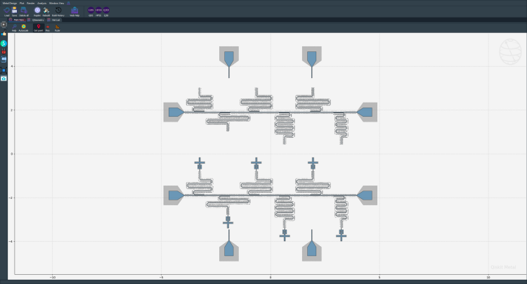
The original design as drawn in the Qiskit Metal GUI (screenshot of the legacy notebook).¶
The rebuild: bare resonators on the upper feedline, resonators with Xmons on the lower one.¶
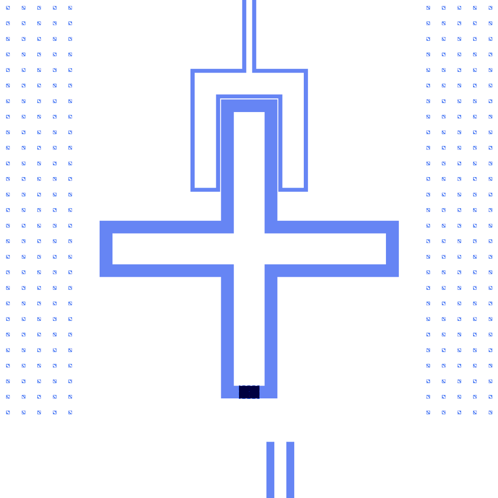
Qubit Q_B1: the Xmon cross with its resonator’s claw above and the junction at the bottom.¶

A launchpad tapering into the left end of the lower feedline.¶
LOM estimates¶
The notebook’s saved LOM output (QuCat normal modes). Target resonator frequencies are in brackets; the lower row sits below target because the qubit claw loads it.
group |
qubit |
f_q (GHz) |
α (MHz) |
resonator |
f_r (GHz) (target) |
κ (MHz) |
χ (MHz) |
|---|---|---|---|---|---|---|---|
Q_B0+R_B0 |
Q_B0 |
5.032 |
-144.3 |
R_B0 |
5.4773 (6.5) |
0.428 |
-3.33 |
Q_B1+R_B1 |
Q_B1 |
5.1264 |
-345.9 |
R_B1 |
5.011 (6.0) |
0.288 |
111 |
Q_B2+R_B2 |
Q_B2 |
5.0445 |
-138.5 |
R_B2 |
4.7145 (5.5) |
0.285 |
-9.1 |
Q_B3+R_B3 |
Q_B3 |
5.0406 |
-146.5 |
R_B3 |
4.3319 (5.0) |
0.225 |
-1.12 |
Q_B4+R_B4 |
Q_B4 |
5.0419 |
-145 |
R_B4 |
4.5254 (5.25) |
0.255 |
-2.66 |
Q_B5+R_B5 |
Q_B5 |
5.0344 |
-146.3 |
R_B5 |
5.845 (7.0) |
0.525 |
-1.35 |
R_T0 |
– |
– |
– |
R_T0 |
6.3569 (6.5) |
0.799 |
– |
R_T1 |
– |
– |
– |
R_T1 |
5.8658 (6.0) |
0.629 |
– |
R_T2 |
– |
– |
– |
R_T2 |
5.3754 (5.5) |
0.485 |
– |
R_T3 |
– |
– |
– |
R_T3 |
4.8838 (5.0) |
0.365 |
– |
R_T4 |
– |
– |
– |
R_T4 |
5.1303 (5.25) |
0.422 |
– |
R_T5 |
– |
– |
– |
R_T5 |
6.8549 (7.0) |
1 |
– |
Q_B1 is hybridised with its resonator (large χ).
These numbers are the notebook’s saved output, not re-run for this page. They are lumped-model estimates (component formulas and calibration), not FEM results; see the LOM page for how far to trust them.
Build spec¶
The rest of this page is the detailed spec the notebook was built from: every component, the changes made while rebuilding, and the notes.
Source: the legacy design notebook components/python/14.0 Two_feedline_resonator_chip.ipynb (Quantum
Metal, DesignPlanar), Quantcore internal. Rebuild: examples/designs/legacy/d14_two_feedline_resonator.ipynb
(+ .json, PNGs), helpers in examples/designs/legacy/_legacy_b.py (d14_plan, flux_hole_runs).
Changes made in the rebuild¶
Die: 10 × 10 mm, confirmed.
Frequencies: the lengths come from bare λ/4 simulations; the bottom (claw-loaded) row sits 0.64–1.09 GHz lower at the same lengths (kept).
Junctions: Metal footprint →
Quantcore Junction(Metal wrapperjunction_type), PDK junction rule (Nb trilayer, Δ = 1.4 meV, I_c·R_n = πΔ/2e = 2.20 mV, R_n 40–50 kΩ, qubits 4–8 GHz; PDK processget_pdk().junction: R_n·A 13.5 kΩ·µm², C_J 50 fF/µm², both assumed by the PDK) at 45 kΩ (L_J 6.73 nH, C_J 15 fF). LOM: f_q ≈ 5.0–5.2 GHz; Q_B1/R_B1 hybridised.The notebook’s JSON was rebuilt from its layout cell. The notebook has not been re-run, so its outputs are cleared and its PNGs may be out of date.
What it is: a resonator characterisation chip. Two straight 20/12 µm feedlines (y = ±1.9 mm) each carry six
λ/4 CPW resonators (10/6 µm), alternating above and below the line at x = −3.25 … +3.25 mm (1.3 mm pitch). The
lengths come from the notebook’s own 1/f = a·L + b calibration (six simulated resonators; R7 and R8 excluded) for
6.50, 6.00, 5.50, 5.00, 5.25, 7.00 GHz left to right. The top feedline’s resonators end open; on the bottom feedline
each open end is the claw of a TransmonCross (Xmon). Eight launchpads: two per edge, ±1.9 mm from each edge centre;
only the left ↔ right pairs carry the feedlines, the top and bottom pads stay unconnected. Custom flux holes (5 µm
squares, 25 µm pitch, ≥ 30 µm from any etch) line the feedlines and the meanders.
Die: 10 × 10 mm, 650 µm sapphire (the source’s size_x/size_y). The rebuild keeps 10 × 10 mm with the PDK v2
die frame drawn on the 10 mm box (the frame is corner-relative); this differs from the 7.5 × 7.5 mm PDK default.
Coordinates below are in the Designer frame (legacy + (5000, 5000)
µm); the legacy mm value is given where useful. Layers: everything on 1/0 (negative mask); the Metal junction
footprint on 2/0 (SIS_junction).
Built (examples/designs/legacy/d14_two_feedline_resonator.ipynb): all Metal cells resolve, every LOM
port maps, all 12 sim groups export.
Plan (legacy §2, §5; _legacy_b.d14_plan() reproduces the legacy printout exactly)¶
Calibration 1/f = 3.082529e-5 · L[µm] + 2.562736e-3 (ε_eff 5.34, ΔL 83.1 µm, RMS 1.13 %).
i |
f (GHz) |
L (µm) |
xc (mm) |
side |
under LP pocket |
N arms |
dy (µm) |
pitch (µm) |
lp (µm) |
open_dx (µm) |
|---|---|---|---|---|---|---|---|---|---|---|
0 |
6.50 |
4910 |
−3.25 |
above |
no |
5 |
1081.0 |
169.3 |
277.4 |
222.6 |
1 |
6.00 |
5325 |
−1.95 |
below |
yes |
4 |
831.0 |
151.3 |
399.4 |
100.6 |
2 |
5.50 |
5815 |
−0.65 |
above |
no |
5 |
1081.0 |
169.3 |
352.8 |
147.2 |
3 |
5.00 |
6405 |
+0.65 |
below |
no |
8 |
1431.0 |
150.7 |
248.6 |
251.4 |
4 |
5.25 |
6095 |
+1.95 |
above |
yes |
5 |
1081.0 |
169.3 |
376.2 |
123.8 |
5 |
7.00 |
4550 |
+3.25 |
below |
no |
8 |
1431.0 |
150.7 |
145.5 |
354.5 |
Rules: the short end sits res_gap = 36 µm from the feedline centre-line (ground strip 36 − 22 − 11 = 3 µm); the
straight coupling section is exactly 500 µm; the open end / claw pin is at x = xc (on the meander’s axis);
x_short = xc − dirx · open_dx with dirx = −1 on the left half (coupler runs towards −x) and +1 on the right half;
y_end = y_short + side · dy. Bend radius 70 µm (legacy §0: 150 µm cannot close in the 1.9 mm pocket).
Components¶
instance |
legacy cell |
catalog ref |
key params (units) |
at (x, y) µm |
rot |
notes |
|---|---|---|---|---|---|---|
|
|
|
pad 400 × 400, pad_gap 240, taper 300, trace 20/12, lead 20 |
(1040, 6900), (1040, 3100) |
0 |
taper tip at legacy (−3.96, ±1.9) mm; the legacy 500 µm lead is drawn as the first 480 µm of the feedline route (same 20/12 CPW), so coupler 0 can run alongside it as in the source |
|
|
|
as above |
(8960, 6900), (8960, 3100) |
180 |
|
|
|
|
as above, lead 500 |
(3100, 1040), (6900, 1040) |
90 |
unconnected in the source |
|
|
|
as above, lead 500 |
(3100, 8960), (6900, 8960) |
270 |
unconnected in the source |
|
|
|
– |
(1750, 8017) |
90 |
legacy (−3.250, 3.017) mm |
|
|
|
– |
(3050, 6033) |
270 |
(−1.950, 1.033) |
|
|
|
– |
(4350, 8017) |
90 |
(−0.650, 3.017) |
|
|
|
– |
(5650, 5433) |
270 |
(0.650, 0.433) |
|
|
|
– |
(6950, 8017) |
90 |
(1.950, 3.017) |
|
|
|
– |
(8250, 5433) |
270 |
(3.250, 0.433) |
|
|
|
cross_length 220, cross_width 50, cross_gap 20; pad |
(1750, 4600) |
180 |
claw pin at (1750, 4217) = the open end; legacy (−3.250, −0.400) mm |
|
|
|
as Q_B0 |
(3050, 1850) |
0 |
claw pin (3050, 2233) |
|
|
|
as Q_B0 |
(4350, 4600) |
180 |
claw pin (4350, 4217) |
|
|
|
as Q_B0 |
(5650, 1250) |
0 |
claw pin (5650, 1633) |
|
|
|
as Q_B0 |
(6950, 4600) |
180 |
claw pin (6950, 4217) |
|
|
|
as Q_B0 |
(8250, 1250) |
0 |
claw pin (8250, 1633) |
|
|
|
5 µm holes, 25 µm pitch, |
per run |
0 |
feedline rows only (see Simplifications) |
– |
|
hanger |
– |
the short ends below |
– |
the route’s hanger end is the short |
The Xmon junction is the legacy gds_cell_name='JJ_grad' cell from an external GDS library (not in the repo); the
Metal wrapper draws the junction line footprint on 2/0 instead. Junction values are not in the source: Lj = 10 nH
(TransmonCross default hfss_inductance, which the legacy design inherits), Cj = 2 fF assumed.
Routes¶
route |
from → to |
type, length (µm) |
hanger (s, length, side, ground_gap, direction) |
short end (x, y) |
notes |
|---|---|---|---|---|---|
|
|
cpw 20/12, 7880 |
– |
– |
y = 6900 |
|
|
cpw 20/12, 7880 |
– |
– |
y = 3100 |
|
|
meander 10/6, 4910 |
(662.6, 500, left, 3, forward) |
(1972.6, 6936 / 3136) |
coupler x ∈ [1472.6, 1972.6] |
|
|
meander, 5325 |
(1840.6, 500, right, 3, forward) |
(3150.6, 6864 / 3064) |
[2650.6, 3150.6] |
|
|
meander, 5815 |
(3187.2, 500, left, 3, forward) |
(4497.2, 6936 / 3136) |
[3997.2, 4497.2] |
|
|
meander, 6405 |
(4588.6, 500, right, 3, backward) |
(5398.6, 6864 / 3064) |
[5398.6, 5898.6] |
|
|
meander, 6095 |
(6016.2, 500, left, 3, backward) |
(6826.2, 6936 / 3136) |
[6826.2, 7326.2] |
|
|
meander, 4550 |
(7085.5, 500, right, 3, backward) |
(7895.5, 6864 / 3064) |
[7895.5, 8395.5] |
s is measured from the feedline start (the LP_L*.tie at x = 1060). Each resonator route: open end / claw →
straight towards the feedline at x = xc → (meander on that segment) → over to the coupler’s far end → 500 µm
coupler → short. Bend radius 70 µm.
Launchers, pads, test structures, markers, labels¶
Eight Metal launchpads (above);
in= the wirebond pad. The four top/bottom pads are unconnected (as in the source).Flux holes: legacy §8 places 5884 holes (2 feedline groups + 12 meander groups, 4 rows per meander following the trace). Rebuilt: the two feedline rows per feedline (±54.5 µm from the centre-line, x ∈ [1040, 8960]) with the legacy filter (hole ≥ 30 µm from every etched edge, applied to the built qcc geometry).
PDK v2 die frame on the 10 mm box; device ID
D14.
LOM node structure¶
FL_T,FL_B: one node each (feedline + both launchpad pads), 50 Ω port at each end.Top resonators: λ/4
TLresfrom the open end node (open_Ti.end) to ground, HANGER κ toFL_T.Bottom:
Q_Biisland (C to ground, JJ to ground) ─ C_g ─ claw nodeQ_Bi.a(C to ground) ─ λ/4TLresR_Bito ground, HANGER κ toFL_B.Unconnected launchpads (
LP_TL,LP_TR,LP_BL,LP_BR): their own pad node with a 50 Ω port.No couplings between resonators (closest pair 201 µm apart in the source).
Targets¶
R_Ti, R_Bi: f = 6.50, 6.00, 5.50, 5.00, 5.25, 7.00 GHz (i = 0…5), from the legacy calibration of the bare
resonator. No qubit targets in the source.
Simplifications for a first rebuild¶
Meanders: the qcc router puts a KQC
Meanderon the straight drop at x = xc (arm count chosen by KQC), instead of Metal’sRouteMeander(N arms of the planned pitch,asymmetry= ±lp). Same total length, same 500 µm coupler, same short and open-end positions; the meander footprint differs slightly (arm count and width).Flux holes: feedline rows only; the 4 rows per meander that follow the trace are left out (
FluxHoleArrayis rectangular; one instance per hole would mean ~4900 instances).Launchpad lead: 20 µm on the four connected pads, the rest of the 500 µm lead is the feedline route (identical CPW), so the hanger of resonator 0 can sit next to it.
Junction: the
JJ_gradcell (external GDS) is replaced by the Metal junction footprint.