Wafer assembly
Wafer assembly packs square dies on a round wafer, names every die and puts a chip layout on each one. The result is one wafer OAS file with the wafer outline, the die labels, the alignment marks and your chips. Use it when a set of chips goes to the fab on one wafer, or when you want to know how many dies of a given size fit.
The code is quantcore_circuits.layouts.wafers.wafer (class Wafer). The demo notebook is
examples/wafer/wafer_assembly.ipynb.
A first wafer
from quantcore_circuits.layouts.wafers.wafer import Wafer

w = Wafer(diameter_mm=100, die_mm=7.5)        # 4 inch, dense, notch on the bottom edge
print(w.die_count)                            # 100
w.write("build/wafer/wafer.oas", chips="examples/designs/legacy/chip_06_test_cyro_tlq.json")
print(w.table_markdown(limit=5))              # die, size, centre, chip
write builds the wafer, writes the OAS and a .csv with the same die table next to it.
Parameters
All lengths are in mm. The layout itself is written in µm, like every other Quantcore layout. The wafer centre is the origin, x points right, y points up.
Parameter |
Default |
Meaning |
|---|---|---|
|
100 |
wafer diameter: 100 (4 in) and 150 (6 in) are the presets, any value works |
|
7.5 |
die side (square): 5, 7.5, 10 or any size |
|
0.1 |
dicing street between neighbouring dies |
|
3.0 |
edge exclusion: no die closer than this to the rim, the notch or the flat |
|
|
|
|
|
|
|
|
|
|
none |
radius of the packing circle, needed for |
|
(0, 0) |
x, y shift of the packing centre from the wafer centre |
|
|
how the die grid sits on the packing centre: |
|
none |
mixed die sizes: |
|
on |
draw a thin frame and the name of every die on 501/0 |
The two packings
Dense fills the whole wafer. A die is placed where it lies completely inside the usable disc: the wafer radius
minus edge_mm, and clear of the notch (the notch is cut out of the outline before the edge exclusion is applied).
Centred fills only a circle of radius_mm around the packing centre (the wafer centre plus offset_mm). A die
counts when all four corners are inside that circle and it is also inside the usable disc. The die grid is laid out
around the packing centre, so the pattern follows the offset. Use it for a small run in the middle of the wafer, or
a run away from a bad wafer region.
Mixed sizes (bands): rows of one die size are stacked from top to bottom, the stack is centred on the packing
centre, and each row takes as many dies as fit. The demo uses [(5, 2), (7.5, 2), (10, 3), (7.5, 2), (5, 2)].
Naming
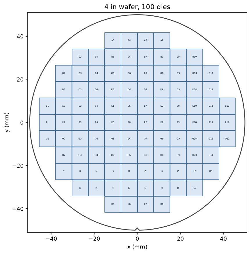
Rows are letters from the top (A, B … Z, AA …), columns are numbers from the left (1, 2 …). A die is
<row><column>, for example F7.
On a one-size wafer the column number counts from the leftmost occupied column of the whole wafer, so a short top row starts at a higher number, like a wafer map. On a mixed wafer the rows do not share a grid, so each row is counted from its own leftmost die.
Layers
Layer |
PDK name |
What is drawn on it |
|---|---|---|
500/0 |
|
the wafer outline: a 200 µm ring just inside the rim, with the notch or flat |
501/0 |
|
die labels and thin die frames, and a small cross at each axis point in the edge band (alignment and orientation marks; none at the notch) |
The chips keep their own layers. Earlier versions of the PDK used 500/0 and 501/0 for these two; the layer map is on the PDK page.
Placing chips
chips= takes a source for the dies:
Value |
Meaning |
|---|---|
one source |
the same chip on every die |
|
by die size in mm ( |
|
by die name |
|
a function of the die |
A source is a design .json (built headless), an .oas / .gds file, or a BuildResult from
quantcore_circuits.assembly.build. Each distinct chip is loaded once and placed as a sub-cell. The chip is centred on
its die using its 100/0 chip boundary; a chip larger than its die raises an error. Dies without a chip stay empty
(label and frame only). The design JSON files are only read.
Pictures
Wafer.plot_map(path) draws the die map (outline, notch, names) with matplotlib. KLayout pictures come from
quantcore_circuits.live.snapshot.snapshot(oas, png, box=...); box (µm) zooms to a region. Both are used in the
notebook.
Four inch
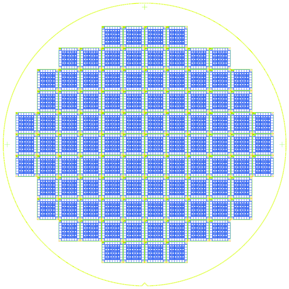
Dense, 7.5 mm dies, 100 dies, the Quantcore cryogenic test chip on every die. The notch is at the bottom.
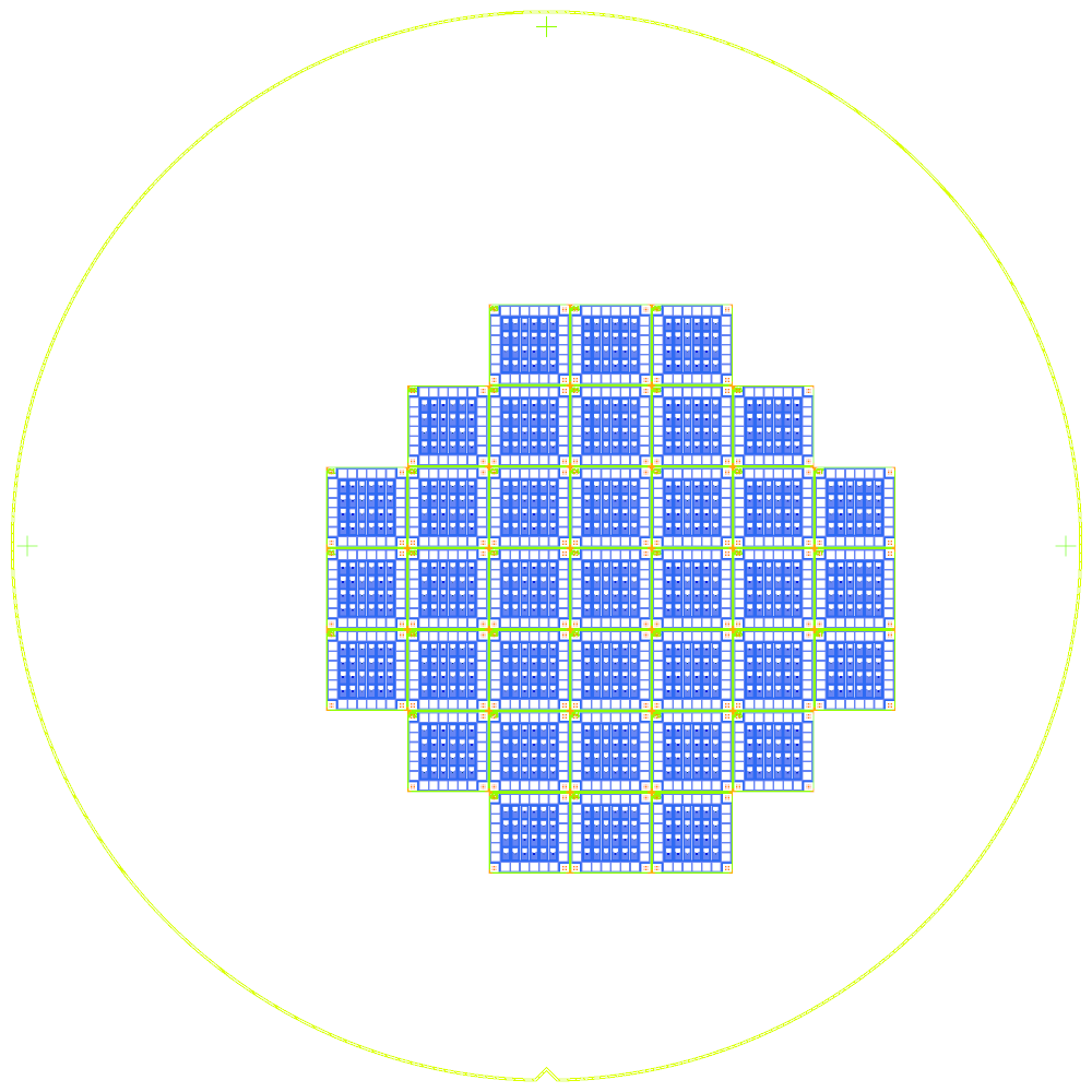
Centred, radius 30 mm, offset (6, -4) mm: 37 dies.
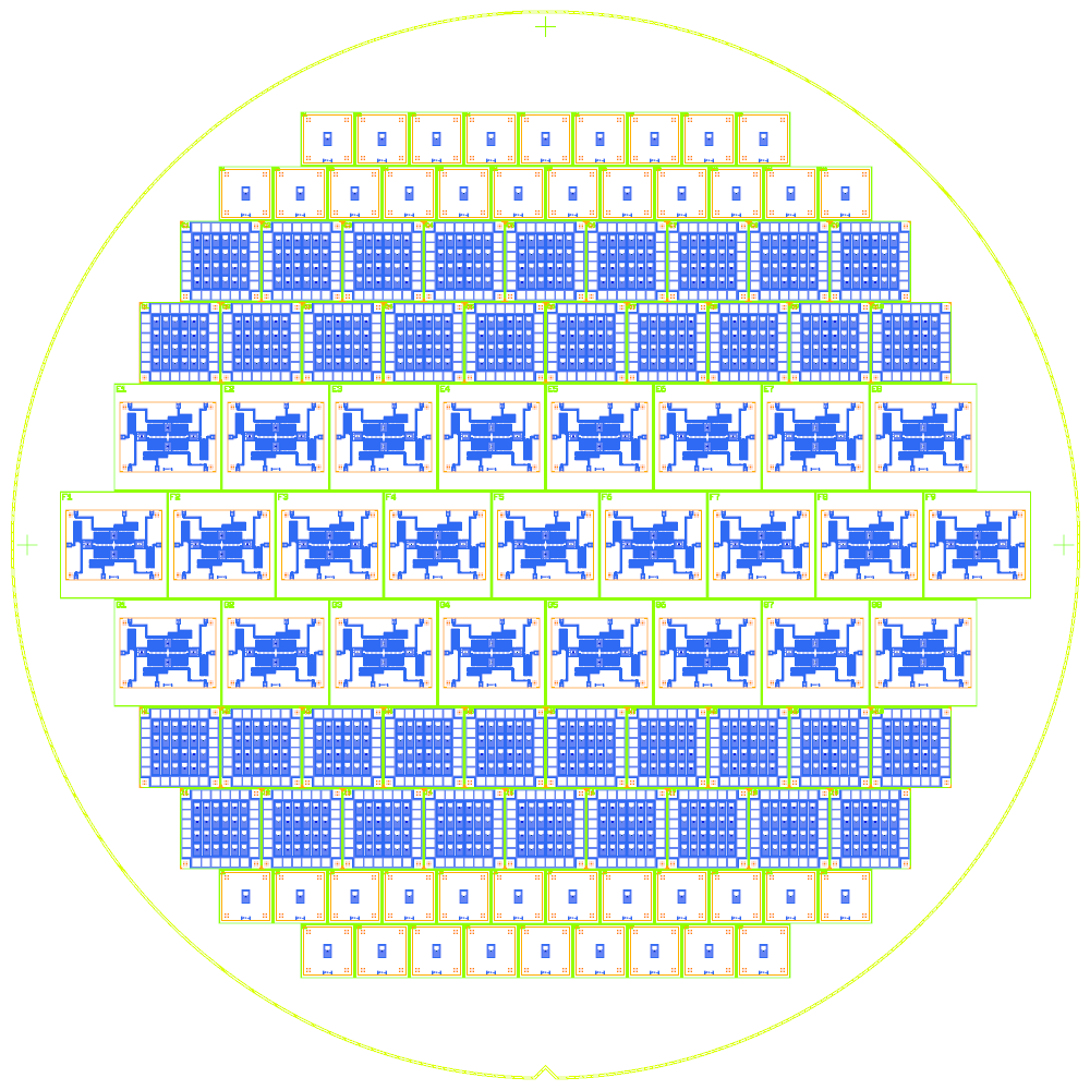
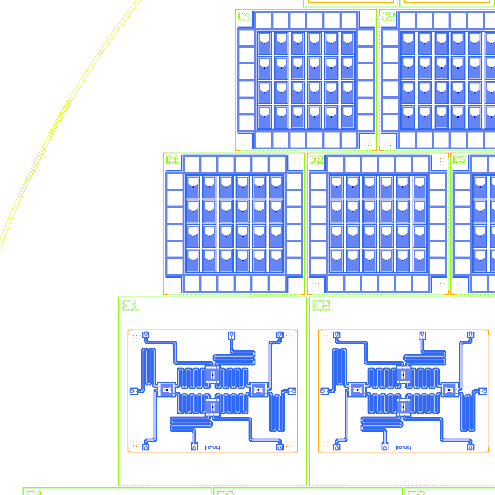
Mixed sizes: 42 dies of 5 mm, 38 of 7.5 mm, 25 of 10 mm (105 dies). The three chips are a 4.5 mm test-pad chip, the cryogenic test chip and the Metal four-qubit chip (9.0 x 6.5 mm).
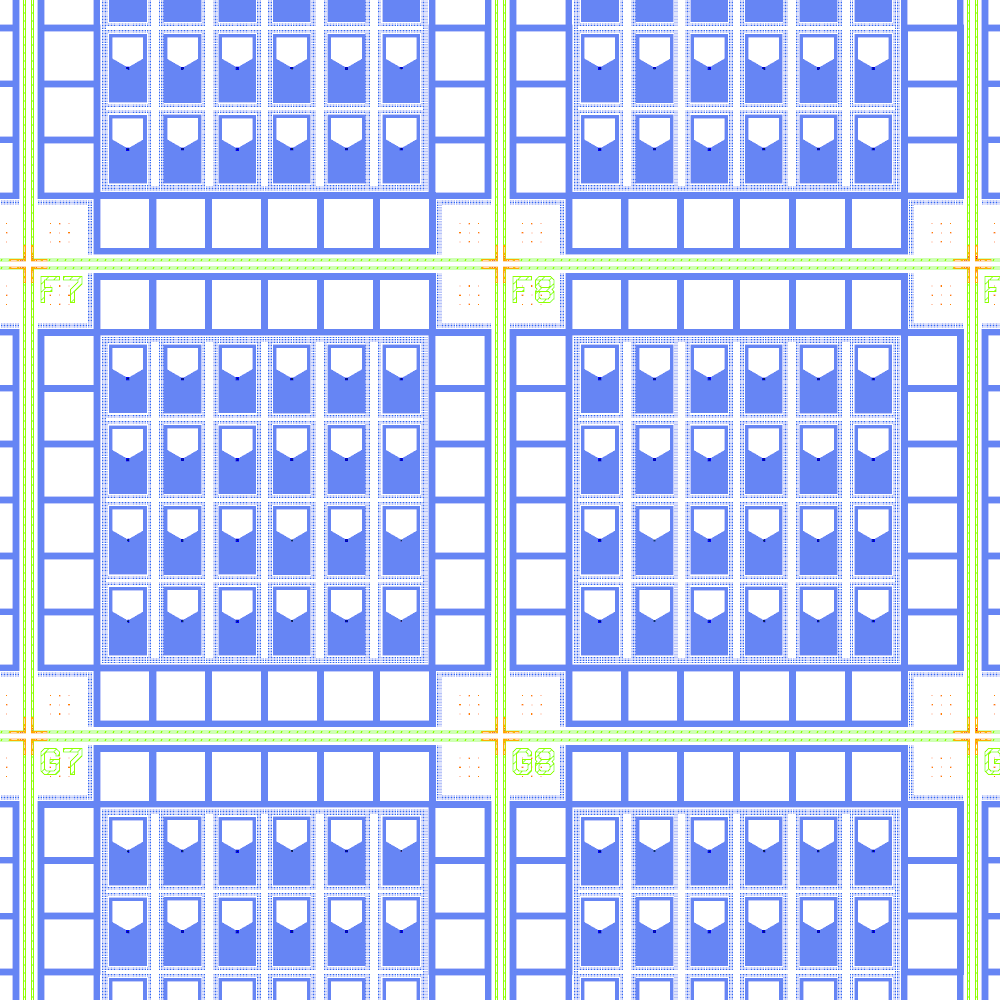
A zoom on two dies: the label is the top-left corner of the die on 501/0, the green frame is the die outline.
Six inch
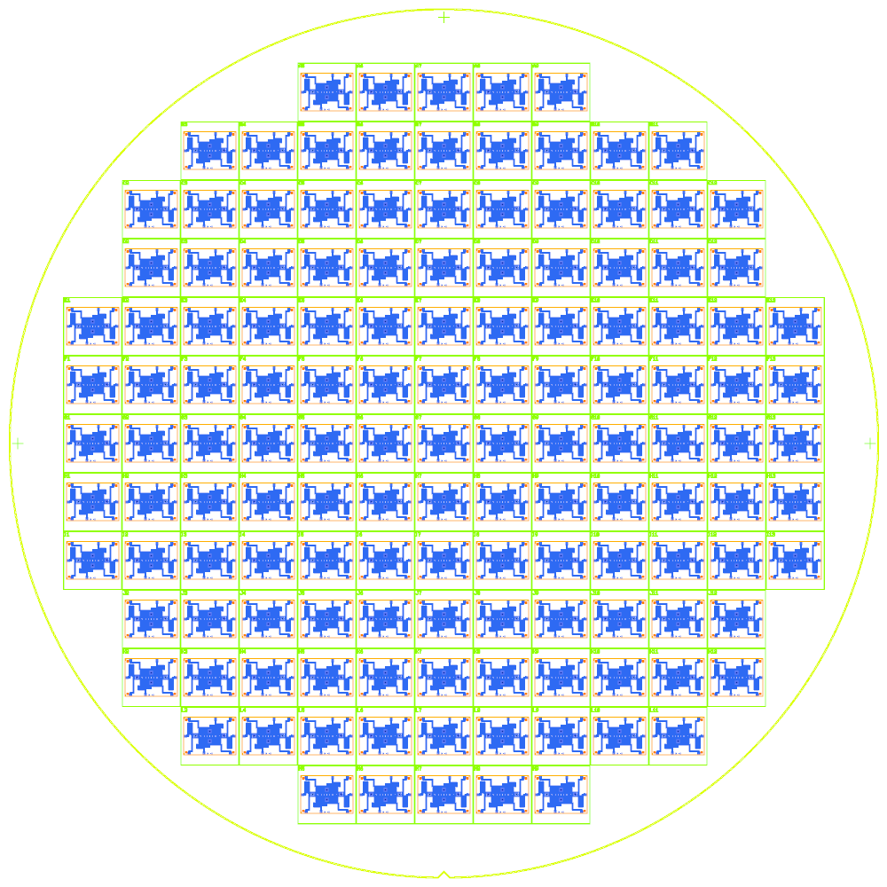
150 mm wafer, dense, 10 mm dies: 137 dies with the Metal four-qubit chip on each.
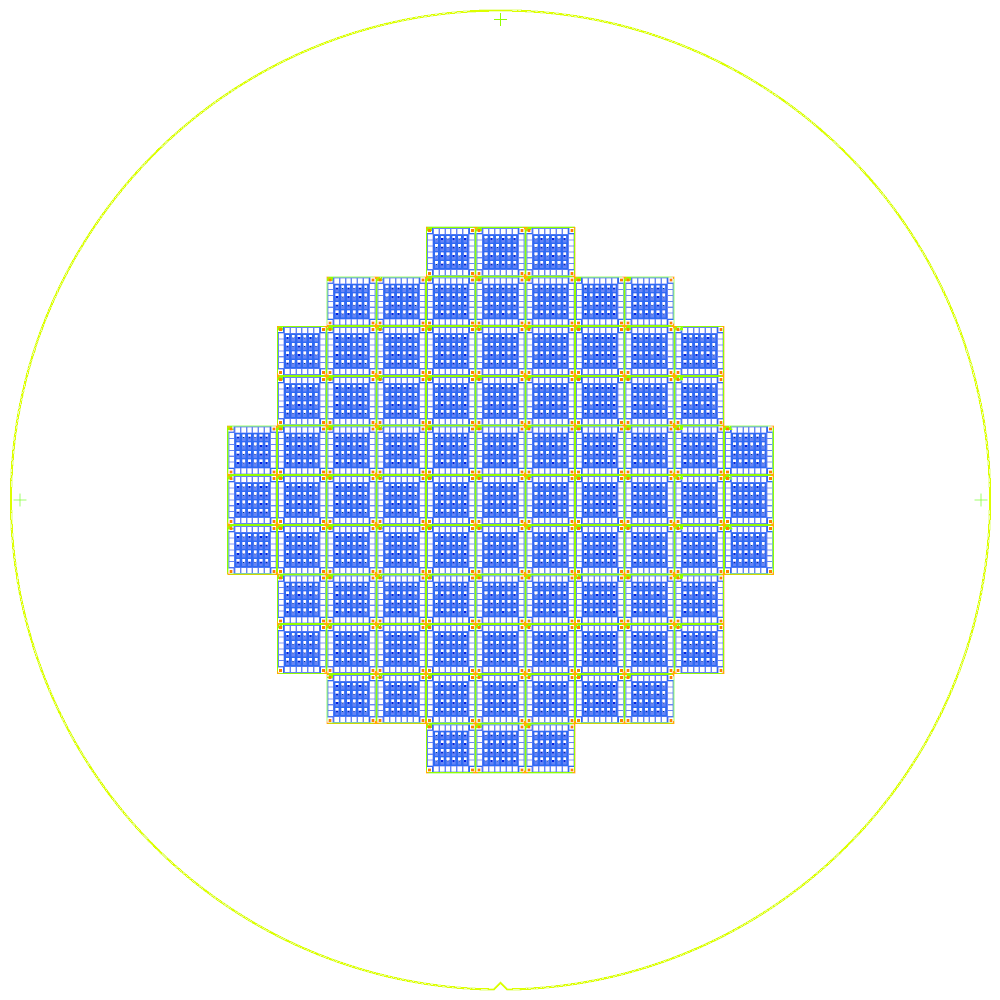
150 mm wafer, centred, 7.5 mm dies, radius 45 mm: 89 dies.
Die counts
Edge exclusion 3 mm, street 0.1 mm, notch at the bottom.
Wafer |
Die |
Packing |
Dies |
|---|---|---|---|
4 in |
7.5 mm |
dense |
100 |
4 in |
7.5 mm |
centred, radius 30 mm, offset (6, -4) |
37 |
4 in |
5 mm |
dense |
238 |
4 in |
10 mm |
dense |
52 |
4 in |
5 / 7.5 / 10 mm |
bands (2, 2, 3, 2, 2 rows) |
105 |
6 in |
10 mm |
dense |
137 |
6 in |
7.5 mm |
centred, radius 45 mm |
89 |
Run the notebook
cd examples/wafer
QCC_LIVE=0 jupyter lab wafer_assembly.ipynb
It builds the chips headless, writes every wafer to build/wafer/ (OAS, CSV table, PNG pictures) and does not touch
examples/designs/. The tests are pytest tests/test_wafer.py.
Limits
Dies are squares on a regular grid; there is no stepper-field or reticle model.
The notch and flat are cut into the outline and kept clear by the edge exclusion; no SEMI notch tolerances are checked.
The wafer OAS is written by
Wafer.write, not byqcc mask.