Resonators on a serpentine feedline (chip_09)
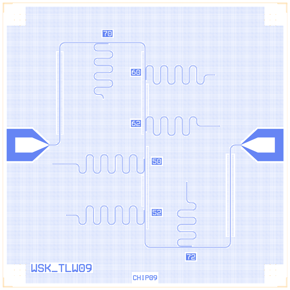
A resonator test chip like chip_07, but with the feedline folded: a 15.7 mm serpentine 10/6 µm line runs from the left pad up, across the top, down the die centre, across the bottom and up to the right pad. Six λ/4 resonators couple to it (one under the top run, four beside the central run, one above the bottom run), targeting 5.0 to 7.2 GHz (labels 50 to 72). The folded feedline lets resonators of very different lengths fit on a 7.5 mm die. Measuring transmission gives their frequencies and quality factors.
It comes from Quantcore’s QWri scripts chip_09_resonatorsExpt.py and its simulation variant chip_09_resonatorsExpt_sim.py (internal). The page covers both variants, each its own notebook. The PDK rebuild adds the die frame, moves the pads to the 100 µm rule and keeps the legacy flux holes. The PDK cheese (5 µm squares with 20 µm gaps, at least 4 µm from the 3/0 keep-outs) now covers the whole die as well. Build them to see long routed feedlines and resonators that differ only in length and coupling.
At a glance
Notebooks |
|
Source |
Quantcore legacy QWri scripts |
Chip |
7.5 × 7.5 mm Quantcore die, sapphire, CPW 10 / 6 µm |
On the chip |
2 bond pads · 1 serpentine feedline · 6 λ/4 resonators · 8 flux-hole arrays |
Pictures
chip_09_resonators_expt (the measured chip)
Resonator targets 7.0, 6.0, 6.25, 5.0, 5.25 and 7.2 GHz (R2, R3, R6, R8, R9, R12). Builds today: yes, rebuilt from its JSON on 2026-11-19 in 2.2 s (the notebook itself was not re-run).
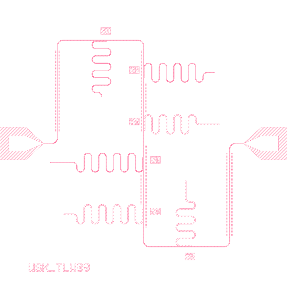
The original legacy layout (render of the legacy GDS).
The rebuild, with the etched labels 50 to 72 (target frequency × 10) and the text WSK_TLW09.

R2 (7.0 GHz) under the top run of the feedline, with its label 70.

The left bond pad and the start of the feedline.
chip_09_resonators_expt_sim (the earlier plan)
The same feedline with an earlier frequency plan (R6 5.0, R8 5.5, R9 5.75 GHz), a different coupling gap on R2 and no labels. Builds today: yes, rebuilt from its JSON on 2026-11-19 in 2.1 s (the notebook itself was not re-run).
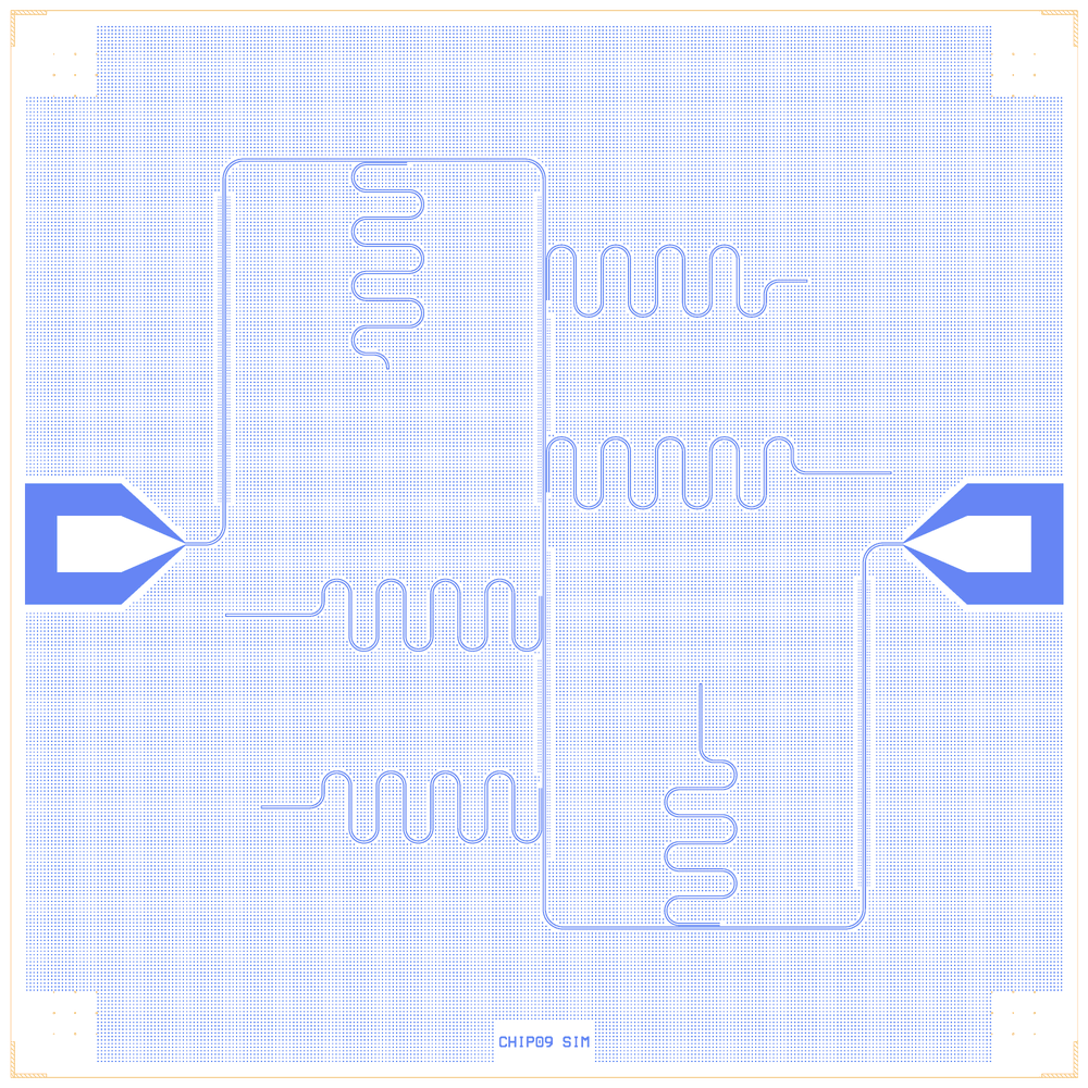
The rebuild of the simulation variant (device ID CHIP09 SIM); the feedline is 161 µm shorter than the original.

R2 beside the top run of the feedline.
LOM estimates
The notebooks’ saved LOM tables (hanger resonators only, no qubits). Target frequencies are in brackets.
chip_09_resonators_expt
resonator |
f_r (GHz) (target) |
κ (MHz) |
|---|---|---|
R2 |
7.1114 (7.0) |
0.222 |
R3 |
6.03 (6.0) |
0.203 |
R6 |
6.3714 (6.25) |
0.239 |
R8 |
5.0613 (5.0) |
0.12 |
R9 |
5.372 (5.25) |
0.143 |
R12 |
7.3699 (7.2) |
0.369 |
chip_09_resonators_expt_sim
resonator |
f_r (GHz) (target) |
κ (MHz) |
|---|---|---|
R2 |
7.104 (7.0) |
0.33 |
R3 |
6.03 (6.0) |
0.203 |
R6 |
5.0613 (5.0) |
0.12 |
R8 |
5.6111 (5.5) |
0.163 |
R9 |
5.8726 (5.75) |
0.187 |
R12 |
7.3699 (7.2) |
0.369 |
These numbers are the notebook’s saved output, not re-run for this page. They are lumped-model estimates (component formulas and calibration), not FEM results; see the LOM page for how far to trust them.
Build spec
The rest of this page is the detailed spec both notebooks were built from: every component, the changes made while rebuilding, and the _sim variant section.
Source: components/python/chip_09_resonatorsExpt.py (create_test_chip, output chip_09_test_res_1.0.oas)
and components/python/chip_09_resonatorsExpt_sim.py (its simulation variant), Quantcore internal. Legacy PCells:
Connector Pad 2, Coupled Resonator, Marker; the feedline is a raw pya.Path. Rebuild:
examples/designs/legacy/chip_09_resonators_expt.ipynb (+ .json, PNGs); tables and the legacy reference in
examples/designs/legacy/_legacy_b.py (C09_*, chip09_reference).
Changes made in the rebuild
_simvariant, rebuilt as its own notebook:examples/designs/legacy/chip_09_resonators_expt_sim.ipynb(designchip_09_resonators_expt_sim, IDCHIP09 SIM): the earlier plan (R6 6200 / R8 5590 / R9 5340 µm, R2 cgap 4, 2 µm shifts, 2-column holes, no labels, no second metal) as a PDK fab chip; the source’s final inversion into a positive 8.5 mm simulation mask is not reproduced (the FEM export does that job). Tables_legacy_b.C09S_RES/C09S_HOLES, referencechip09_sim_reference(). LOM: f_r 5.14–7.49 GHz.Lengths: simulated without claws (bare), as on chip_07.
What it is: a resonator test chip with a long serpentine 10/6 µm feedline (corners rounded at 150 µm,
15663.7 µm) from the left bond pad up, across the top, down the die centre, across the bottom and up to the right
pad. Six Coupled Resonators (λ/4, coupler 299.5 µm at 4–6 µm): one under the top run (R2), four beside the
central vertical run (R3, R6 right; R8, R9 left), one above the bottom run (R12). Targets (comments and the etched
labels “70”, “60”, “62”, “50”, “52”, “72” = f × 10): 7.0, 6.0, 6.25, 5.0, 5.25, 7.2 GHz. Eight flux-hole columns
(3 × n holes); text “WSK_TLW09”.
Die: 7.5 × 7.5 mm, centred on (0, 0) → shifted by (+3750, +3750). The PDK v2 die frame replaces the legacy
Marker corners and the 10/0 boundary boxes. Legacy layers 1/0 (etch), 3/0 (second-metal envelope), 10/0
(boundary and the feedline’s centre path).
Built; XOR with the legacy PCells and path is 0.0 µm² on every pad, resonator, hole array and label, 360 µm² (0.05 %) on the feedline (arc discretisation).
Components
instance |
legacy cell |
catalog ref |
key params |
at (x, y) µm |
rot |
legacy (x, y), notes |
|---|---|---|---|---|---|---|
|
|
|
pad 400 × 450, pad_gap 225, taper 450, trace 10/6, round False |
(1125, 3750) |
270 |
(−2625, 0) rot 3 |
|
|
|
as PL |
(6375, 3750) |
90 |
(2625, 0) rot 1 |
|
|
|
cpw_len 4410, cgap 6, flip False |
(2650, 6422) |
0 |
(−1100, 2672); 7.0 GHz |
|
|
|
cpw_len 5200, flip True |
(3776, 5600) |
90 |
(26, 1850) rot 1; 6.0 GHz |
|
|
|
cpw_len 4920, flip True |
(3778, 4250) |
90 |
(28, 500) rot 1; 6.25 GHz; legacy second metal |
|
|
|
cpw_len 6200 |
(3726, 3250) |
90, mirror |
(−24, −500) rot 1 mirror; 5.0 GHz |
|
|
|
cpw_len 5840 |
(3724, 1900) |
90, mirror |
(−26, −1850) rot 1 mirror; 5.25 GHz; legacy second metal |
|
|
|
cpw_len 4250, flip True |
(4850, 1080) |
180 |
(1100, −2670) rot 2; 7.2 GHz; legacy second metal |
|
hole cell array |
|
5 µm, 3 columns at 15 µm × n rows at 20 µm (n = 108, 108, 108, 40, 40, 108, 108, 108) |
first hole at legacy (−2315, 300), (−2215.5, 300), (−70, 300), (−75, −1600), (40, 800), (45, −2200), (2170, −2400), (2300, −2400) |
0 |
on 1/0 only (the 3/0 copy is commented out) |
|
|
|
“WSK_TLW09”, mag 300 |
(750, 400) |
0 |
(−3000, −3350) |
|
|
|
mag 200, inverted |
legacy (−1100, 2870), (−350, 1850), (−350, 500), (200, −500), (200, −1850), (1100, −3020) |
0 |
the f × 10 labels |
– |
|
PDK die frame |
– |
– |
– |
replaced |
Common resonator parameters: cpw_len 4660 (overridden), gap 6, clength 299.5, cgap 4, width 300, flip False,
neck_length 150, ground True. Second metal (as chip_07): R6, R9, R12 have l = 3/0, fab_l = 1/0; they are drawn on
1/0 here.
Routes
route |
from → to |
type |
waypoints (legacy frame) |
notes |
|---|---|---|---|---|
|
|
cpw 10/6, r = 150 µm, 15663.7 µm |
(−2250, 0), (−2250, 2700), (0, 2700), (0, −2700), (2250, −2700), (2250, 0) |
the legacy raw path; 16050 µm before rounding |
LOM node structure
FL: one node (route + both pads), 50 Ω at each pad.Each
Ri: λ/4TLresfromRi.resto ground + HANGER κ to the feedline, declared against the routed feedline:d.couple("K_Ri", "Ri", "FL")(a C coupling may name a route: its conductor). Same netlist as the earlier declaration against the padPL(whose only node is the feedline’s); κ 0.10–0.31 MHz.No qubits or junctions.
Targets
R2 7.0, R3 6.0, R6 6.25, R8 5.0, R9 5.25, R12 7.2 GHz.
The _sim variant (chip_09_resonatorsExpt_sim.py), rebuilt as chip_09_resonators_expt_sim
An earlier frequency plan of the same chip, written as a simulation mask: the 10/0 device boundary is 8.5 mm, the
markers and the text labels are left out, and the output is positive (device_boundary − etch on 1/0, layers 3/0
and 10/0 deleted, …_sim.oas). The qcc FEM export (C.export_sims) does that job for the rebuilt chip. Differences:
item |
Expt (rebuilt) |
_sim |
|---|---|---|
R2 |
y 2672, cgap 6 |
y 2674, cgap 4 |
R6 |
(28, 500), cpw_len 4920 (6.25 GHz), second metal |
(26, 500), cpw_len 6200 (5.0 GHz) |
R8 |
(−24, −500), cpw_len 6200 (5.0 GHz) |
(−26, −500), cpw_len 5590 (5.5 GHz) |
R9 |
cpw_len 5840 (5.25 GHz), second metal |
cpw_len 5340 (5.75 GHz) |
R12 |
y −2670, second metal |
y −2674 |
flux holes |
3 columns ( |
2 columns ( |
Simplifications for a first rebuild
Second-metal resonators drawn on 1/0; PDK frame instead of the legacy markers.