Seven Xmons and eight resonators (chip_10a)
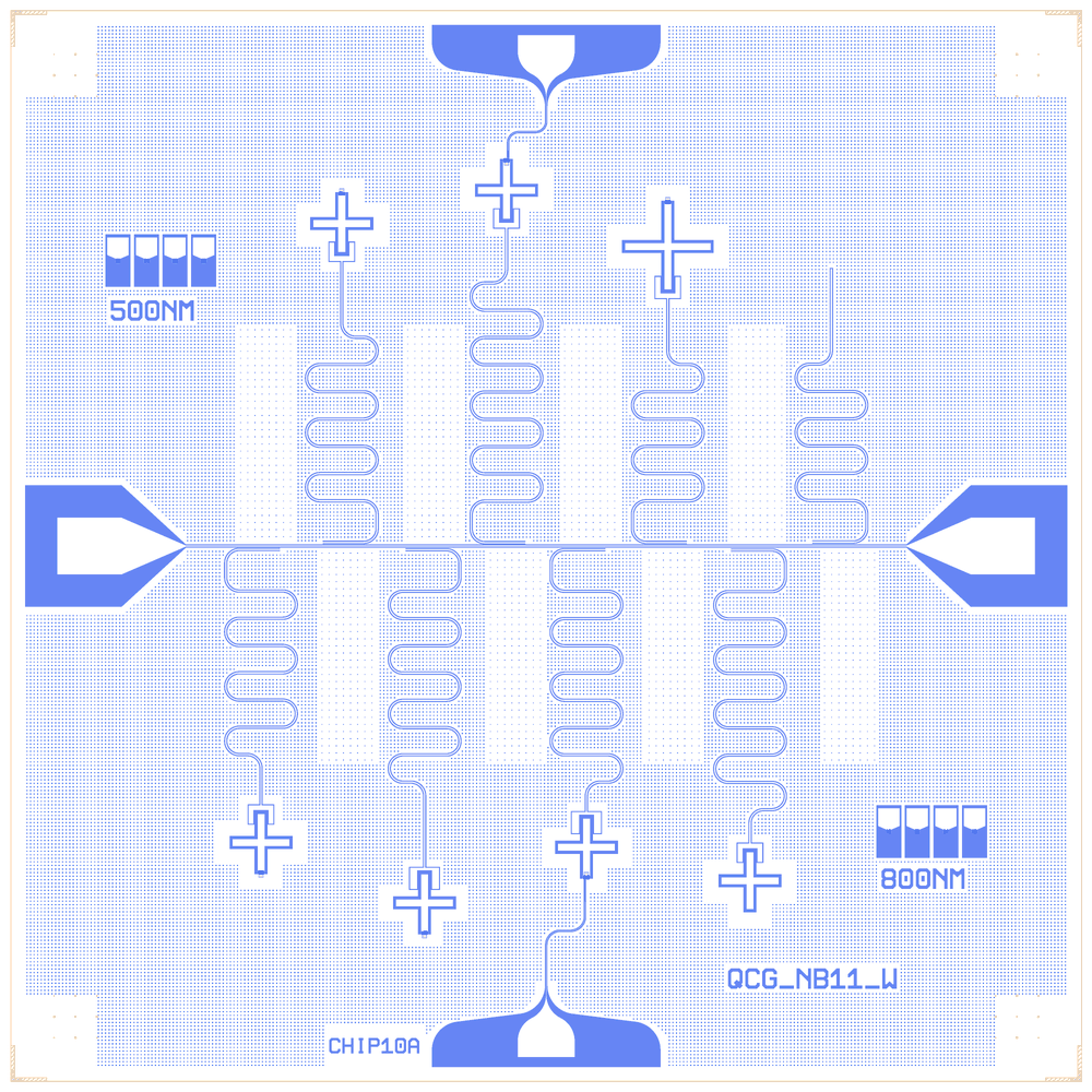
A qubit chip. One feedline crosses the die, eight λ/4 readout resonators hang off it (four above, four below), and seven Xmon qubits sit at the resonators’ open ends, each end wrapped around a qubit’s claw. Two of the Xmons are SQUID qubits that can be tuned with flux; their flux lines come in from two small pads at the top and bottom edge. Small test-junction blocks (labelled 500NM and 800NM), flux-trap holes and the label QCG_NB11_W fill the rest. It was made to measure qubit and resonator frequencies, the coupling between them, and the flux tuning.
It comes from Quantcore’s QWri script chip_10a_flux_TLQubits.py (internal), the revision of chip_05 with new junction scripts, new test pads and a finer flux line. The rebuild is in the PDK die frame (device ID CHIP10A), with junctions on the PDK junction rule and pads on the 100 µm rule. The PDK cheese (5 µm squares with 20 µm gaps, at least 4 µm from the 3/0 keep-outs) also covers the whole die, and the holes drawn in the original layout stay. Build it to see a full qubit chip: claws on resonator tails, flux lines and test junctions on one die.
At a glance
Notebook |
|
Source |
Quantcore legacy QWri script |
Chip |
7.5 × 7.5 mm Quantcore die, sapphire, CPW 10 / 6 µm |
On the chip |
7 Xmons (2 flux-tunable SQUIDs) · 8 λ/4 resonators · 1 feedline with 2 bond pads · 2 flux pads and flux lines · 8 test-pad blocks |
Builds today |
yes, rebuilt from its JSON on 2026-11-19 in 2.6 s (the notebook itself was not re-run) |
Pictures
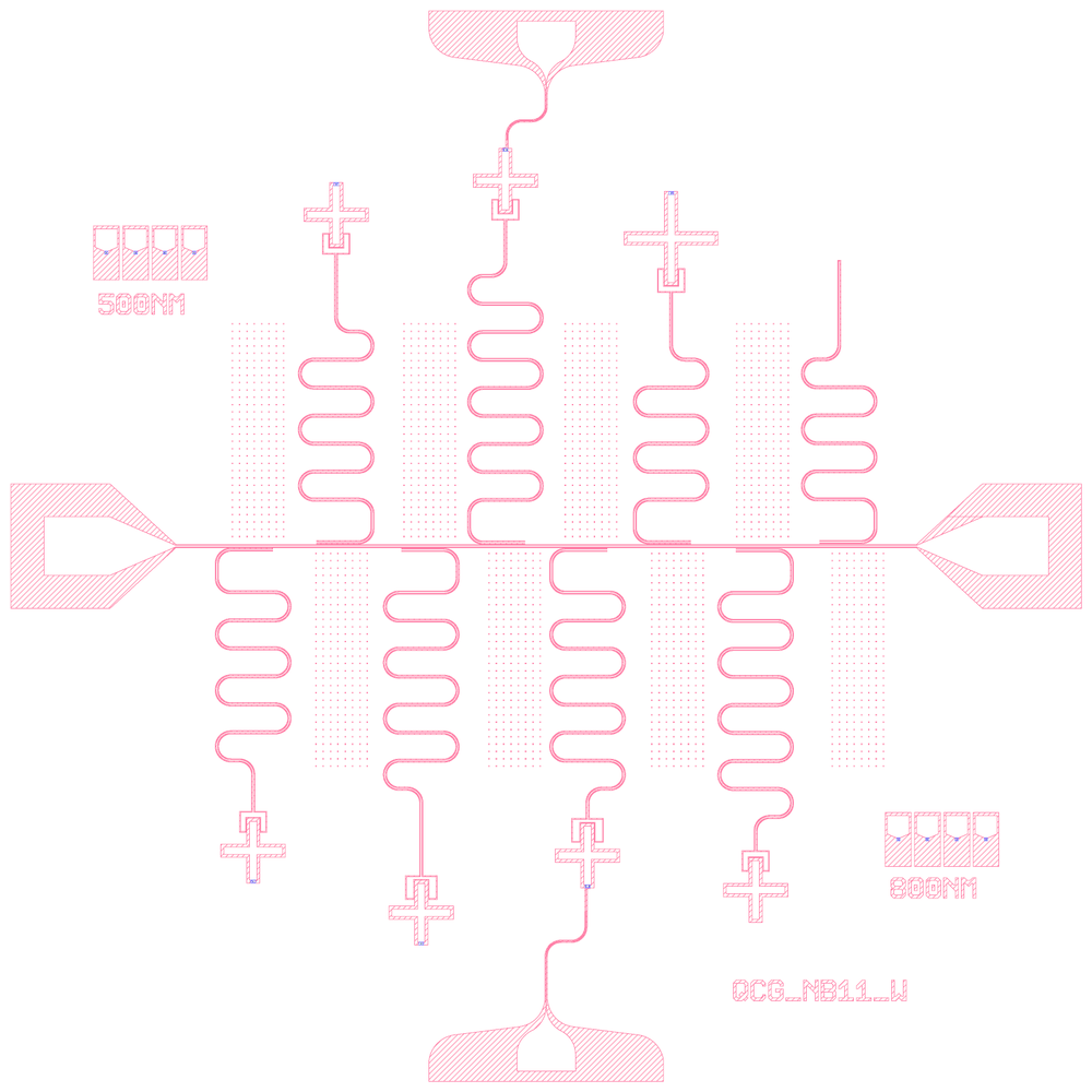
The original legacy layout (render of the legacy GDS).
The rebuild: qubits at the resonator ends, flux pads at the top and bottom centre, test-pad blocks in two corners.
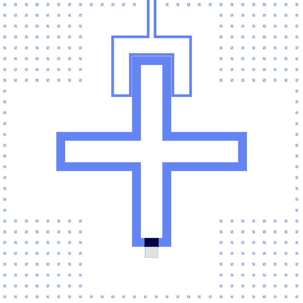
Q1: an Xmon cross with the resonator’s claw around its top arm; the junction is at the bottom end.
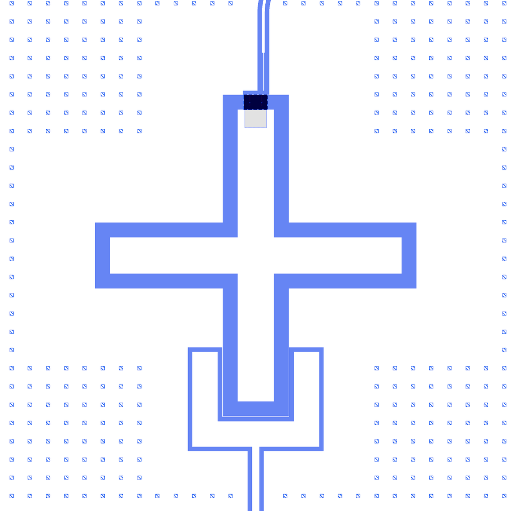
Q4, a SQUID qubit: the claw at the bottom, the flux line arriving at the top.

The top flux pad narrowing into the flux line that runs down to Q4.
LOM estimates
The notebook’s saved LOM table (QuCat normal modes). Target resonator frequencies from the legacy plan are in brackets.
group |
qubit |
f_q (GHz) |
α (MHz) |
resonator |
f_r (GHz) (target) |
κ (MHz) |
χ (MHz) |
|---|---|---|---|---|---|---|---|
Q1+R1 |
Q1 |
5.8776 |
-365.7 |
R1 |
5.7634 (6.5) |
0.146 |
101 |
Q2+R2 |
Q2 |
5.8242 |
-121.8 |
R2 |
5.6272 (6.25) |
0.143 |
75.2 |
Q3+R3 |
Q3 |
5.7949 |
-197.2 |
R3 |
4.9722 (5.5) |
0.101 |
-1.98 |
Q4+R4 |
Q4 |
7.7695 |
-170.3 |
R4 |
4.7226 (5.0) |
0.0883 |
-0.0543 |
Q5+R5 |
Q5 |
7.7506 |
-169.3 |
R5 |
5.3035 (6.0) |
0.122 |
-0.159 |
Q6+R6 |
Q6 |
6.0567 |
-121.7 |
R6 |
6.34 (7.2) |
0.179 |
-7.76 |
R7+Q7 cross |
– |
– |
– |
R7 |
4.8406 (5.25) |
0.0948 |
– |
R8 |
– |
– |
– |
R8 |
6.9626 (7.0) |
0.312 |
– |
Q1 and Q2 are strongly hybridised with their resonators (large χ). The notebook also compares R_n 28.1 kΩ (legacy) with the PDK nominal 45 kΩ for Q6.
These numbers are the notebook’s saved output, not re-run for this page. They are lumped-model estimates (component formulas and calibration), not FEM results; see the LOM page for how far to trust them.
Build spec
The rest of this page is the detailed spec the notebook was built from: every component, the changes made while rebuilding, and the notes.
Source: components/python/chip_10a_flux_TLQubits.py (create_test_chip(), writes
chip_10a_flux_TLQubits_1.0.oas), Quantcore internal. Notebook: examples/designs/legacy/chip_10a_flux_tlqubits.ipynb.
Changes made in the rebuild
Junction indexing fixed as on chip_05 (same
bot[i-1]loop): Q1–Q5 js 5, Q6 js 8.Flux-line corners: FLUX4 r = 75 µm, FLUX5 r = 100 µm (largest that fit; was 50). Q4 orientation: confirmed.
Junctions: legacy xjc trilayer cells at the legacy fingers on the PDK junction rule (Nb trilayer, Δ = 1.4 meV, I_c·R_n = πΔ/2e = 2.20 mV, R_n 40–50 kΩ, qubits 4–8 GHz; PDK process
get_pdk().junction: R_n·A 13.5 kΩ·µm², C_J 50 fF/µm², both assumed by the PDK). LOM: Q1/R1 and Q2/R2 hybridised.claw_tail_gap= 6 µm (legacycap_spacing).The notebook’s JSON was rebuilt from its layout cell. The notebook has not been re-run, so its outputs are cleared and its PNGs may be out of date.
What it is: a revision of chip_05 (docs/designs/legacy/chip_05_flux_tlqubits.md): the same layout
idea (feedline between two pads, eight Coupled Resonators alternating above/below, seven Xmon Crosses whose
claws take the resonator tails, Q4/Q5 as SQUIDs with flux lines from two small pads at the top/bottom edge centres,
flux-trap holes, junction test pads, labels) with new junction scripts (xjc_junction_TL_mod /
xjc_squid_TL_mod: the trilayer cells the TrilayerJunction / TrilayerSquid golden tests use), new test pads
(eight xtp_testpads_TL_small), Connector Pad 2 feed pads, a 4/6 µm flux line with a 1 µm tip, finer flux holes,
and resonator couplers at three strip widths. Everything below is the delta to the chip_05 spec; what is not listed
is as chip_05.
Die: 7.5 × 7.5 mm, centred on (0, 0) → (+3750, +3750); PDK v2 die frame instead of the legacy Marker corners
and 10/0 boundary. HSQ corner markers (500/0, fab_l 150/0, thickness 50, width 150) at the four corners, as chip_05 → CornerMarker(hsq=True). Pads at all four edge centres again → the
automatic device ID slides along the bottom edge to a free spot (CHIP10A).
Built (examples/designs/legacy/chip_10a_flux_tlqubits.ipynb, derived from the chip_05 notebook).
Etch XOR 0 on every instance, junction windows included (Q1–Q6 were 600 µm² each with the windows off; on now,
and the FEM export drops the window), except the flux-line corners (r = 50 vs 100 µm); junction-layer XOR 0 except Q4 (the
legacy SQUID there is upside down, see the notebook). Flux tip: Xmon defaults (flux_x −10.5, tip 0.5, slot 28 × 5)
a 1 µm-wide last route section (
waypoint(a=1, b=7.5, taper_length=1)); Q2/Q6mirror_squid= the legacy flag.
Components (legacy frame, µm), delta to chip_05
instance |
legacy → catalog ref |
params |
at |
rot / mirror |
|---|---|---|---|---|
FL |
Coplanar Waveguide → |
length 7500 − 2000 − 40 − 210 = 5250, gap 6 ( |
(0, 0) |
0 |
PL, PR |
Connector Pad 2 → |
400 × 450, pad_gap 225, taper 450, 10/6, round False, sim False (chip_07’s pads) |
(∓2625, 0) |
270° / 90° |
PFT, PFB ( |
Connector Pad → |
|
|
as chip_05 (names swapped vs position) |
R1 … R8 |
Coupled Resonator → |
common gap 6, clength 300, cgap 4, width 304, neck 400, ground False; cpw_len 4740 / 4920 / 5590 / 6000 / 5200 / 4250 / 5840 / 4500; flip R2, R3, R7, R8; R8 ground True (end cap; chip_05’s CUT8 box is gone) |
x = −2000, −1430, −850, −280, 280, 850, 1430, 2000; y = −(22+2), +(22+4), −(22+4), +(22+2), −(22+4), +(22+4), −(22+6), +(22+6) |
mirror True above |
Q1 … Q7 |
Xmon Cross → |
Q1/Q2/Q4/Q7 |
(−1998, −2077), (−1432, 2259), (−852, −2500), (−278, 2492), (282, −2110), (852, 2098), (1428, −2345) |
rot 0 / 2 alternating (Q1 0, Q2 2, …) |
junctions |
|
|
(x, y ± 200 ± gap/2) with gap 20 → y ± 210; Q6 + 100 |
mirror flag: Q1 F, Q2 T, Q3 F, Q4 F, Q5 F, Q6 T (the SQUID branch toggles it twice) |
FLUX4, FLUX5 |
raw paths, 4 µm centre / 6 µm gaps, corners rounded at 100 µm, + 1 µm-wide tip + 28 × 5 µm ground box |
top: (0, 3155) → (0, 3000) → (−267, 3000) → (−267, 2770), tip to (−267, 2712.5), box centred at (−281.5, 2715); bottom: (0, −3155) → (0, −2795) → (271, −2795) → (271, −2490), tip to (271, −2330.5), box at (285.5, −2333) |
as chip_05 (routes |
|
H0 … H7 |
hole array → |
5 µm holes at 50 µm pitch, nx = int(400/50) = 8, ny = int(1500/50) = 30 (on 1/0 and 3/0) |
first hole at (x − 50, y): x = −2090, −1520, −920, −340, 180, 770, 1350, 2000; y = 65 / −1500 alternating |
0 |
TP1 … TP8 |
|
bf 0.5 (TP1–4), 0.8 (TP5–8) |
(−3000, 2000), (−2800, 2000), (−2600, 2000), (−2400, 2000), (3000, −2000), (2800, −2000), (2600, −2000), (2400, −2000) |
0 |
labels |
|
“500nm” at (−3050, 1580), “800nm” at (2350, −2400), “QCG_Nb11_W” at (1275, −3100) |
0 |
|
CLEARER |
30 × (20 + 25) µm boxes cut from 1/0 and 3/0 at every junction (Q1–Q6) |
|
(x, y ± 200 ± 10 ± 12.5); Q4/Q5 shifted ∓25 (“for squids cut inside”); Q6 + 100 |
LOM node structure
As chip_05: FL.line (50 Ω at each pad) ─ HANGER K_Ri ─ Ri.res λ/4 (shorted at the coupler) ─ tail joined to
Qi.claw_n (wire coupling) ─ C_g ─ Qi island (JJ / SQUID to ground; Q7 none). FLUX4/FLUX5 → control:flux of
Q4 / Q5. R8 plain (open end cap, no qubit).
Targets
Source comments: R4 “5 GHz, reduced 200 µm for this flux, should shift a bit right”; otherwise as chip_05 (R1 6.5, R2 6.25, R3 5.5, R5 6, R6 7.2, R7 5.25, R8 7 GHz).
Simplifications for a first rebuild
As chip_05 (frame; flux-line tip geometry through the Xmon flux-port parameters; labels as TextLabel).