Fab-ready 4-qubit chip (SQuADDS)
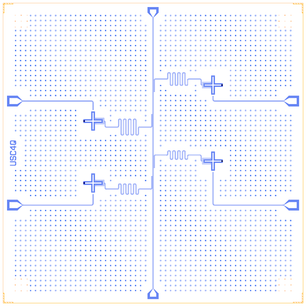
Four identical grounded cross transmons on a 5 × 5 mm chip, each with a λ/4 readout hanging on one vertical feedline and a charge line of its own. It is the “fab-ready” chip of SQuADDS tutorial 5 (USC4Q_qff2024, MIT), rebuilt on the Quantcore PDK. The readouts are staggered over 5.48 to 8.48 GHz.
Build this one to learn four hanger readouts on one feedline, charge lines that end open next to a qubit, and junctions sized from a frequency target by the PDK rule.
At a glance
Notebook |
|
Source |
SQuADDS tutorial 5 and its exported |
Chip |
7.5 × 7.5 mm Quantcore die, the source’s 5 × 5 mm chip centred in it, feedline 11.7 / 5.1 µm |
On the chip |
6 Metal launchpads · 1 feedline · 4 cross transmons · 4 λ/4 hanger readouts · 4 charge lines |
Builds today |
yes (layout built on 2026-11-19 in 8 s) |
How the notebook builds it
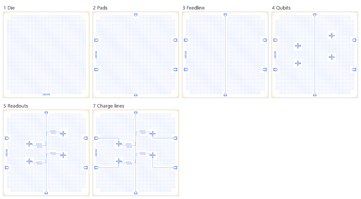
Die. The Quantcore die with the frame and the device ID
USC4Q.Bond pads. Two feedline pads and four charge-line pads, on the 100 µm pad rule.
Feedline. A straight line from the top pad to the bottom pad.
Qubits. The junction sized for the PDK band’s floor (4.05 GHz), and four cross transmons.
Readouts. Four λ/4 hangers with an 8-turn meander and a 325 µm coupled section.
Coupling. None: the qubits do not couple to each other.
Charge lines. One line per qubit, turning once and ending open 284 µm from the qubit centre.
Whole chip. Targets, one sim group per qubit, centring, save.
LOM estimates
Numbers are from a run of this notebook on 2026-11-19 (Setup, Design, Check and the LOM cells, 8 s): QuCat normal modes with QuTiP dressed values.
group |
qubit |
f_q (GHz) |
α (MHz) |
resonator |
f_r (GHz) |
κ (MHz) |
χ (MHz) |
|---|---|---|---|---|---|---|---|
Q1R1 |
Q1 |
4.088 |
-213 |
R1 |
6.119 |
0.101 |
-0.381 |
Q2R2 |
Q2 |
4.088 |
-213 |
R2 |
6.993 |
0.148 |
-0.275 |
Q3R3 |
Q3 |
4.088 |
-213 |
R3 |
7.816 |
0.203 |
-0.228 |
Q4R4 |
Q4 |
4.088 |
-213 |
R4 |
8.591 |
0.265 |
-0.204 |
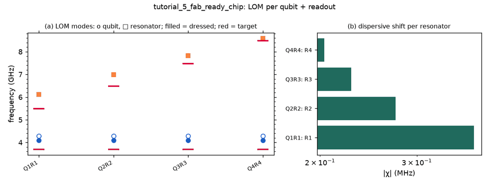
These are lumped-model estimates from component formulas and calibration, not FEM results. The LOM page says how far to trust them.
Build spec
The rest of this page is the detailed spec the notebook was built from: every component, port, route and length.
Source: tutorials/Tutorial-5_Designing_a_fab_ready_chip_with_SQuADDS.ipynb
and its exported GDS tutorials/gds_files/USC4Q_qff2024.gds (173 kB). The GDS was read with a KLayout script to recover
the numbers the notebook does not print. Licence MIT (“Copyright (c) 2023 Sadman Ahmed Shanto”, verified; the notebook
footer says © Shanto & Levenson-Falk 2024, MIT) · read on 2026-11-02. Built with Quantum Metal plus SQuADDS TransmonCross.
What it is: 4 identical grounded cross transmons (one SQuADDS DB design) on a 5 × 5 mm chip. Each has a λ/4 meander
coupled to a straight vertical feedline through a CoupledLineTee, and a charge line ending in an open 50 µm past the
cross pocket. The resonators are “sprayed” over 5.48–8.48 GHz so that one lands on ω₀₂ despite ±0.75 GHz junction spread.
Measured in transmission (2 feedline pads + 4 charge pads = 6 ports, for a 5.4 mm board cut-out).
Frame: source centred, chip 5 × 5 mm. Box (0, 0, 5000, 5000), Designer = source + (2500, 2500). Feedline CPW
11.7/5.1 µm, resonators 11.7/(5.1 assumed) µm, charge lines 10/6 µm. GDS layers: 3 = metal, 6 = charge lines and
their pads (a fab request in the tutorial), 20/60 = Dolan junction, 3/2 = cheese holes.
A first build uses Xmon, BondPad and hanger routes.
Components
instance |
catalog ref |
key params (units) |
at (x, y) Designer |
rot |
notes |
|---|---|---|---|---|---|
Q1 |
|
cross tip-to-tip 420 (Metal cross_length 210), arm_width 30, gap 30. One claw toward the feedline: claw trace 15, finger length ≈190 (back along the arm), claw to cross ≈39 |
(1000, 3300) |
claw faces +x |
source (−1500, 800), Metal orientation −90 |
Q2 |
|
same |
(4000, 4200) |
claw faces −x |
(1500, 1700), orientation 90, JJ flipped |
Q3 |
|
same |
(1000, 1750) |
+x |
(−1500, −750) |
Q4 |
|
same |
(4000, 2300) |
−x |
(1500, −200) |
P_TOP |
|
(2500, ≈4700), port at (2500, 4575) |
180 (faces S) |
wb_top, Metal pos_y 2.1 mm |
|
P_BOT |
|
(2500, ≈300), port at (2500, 625) |
0 (faces N) |
wb_bottom, pos_y −1.9 mm |
|
LP1 / LP3 |
|
(500, 3800) / (500, 1200) |
270 (faces E) |
source (−2000, ±1300) |
|
LP2 / LP4 |
|
(4500, 3800) / (4500, 1200) |
90 (faces W) |
source (2000, ±1300) |
Junction: Dolan, L_J = 15.904 nH (from the DB entry), J_c 0.25 µA/µm², 200 nm × 420 nm, so
junction={"Lj_nH": 15.9, "Cj_fF": 2} (Cj assumed). All four use the same Lj.
Routes
FL runs from P_TOP.a (2500, 4575) to P_BOT.a (2500, 625), travelling −y. Left is +x (east), so west qubits (Q1, Q3)
are right and east qubits are left. CLT coupled section, measured in the GDS: a 325 µm straight, coupled-trace
centre 29.8 µm from the feedline centre, shorted far end (open_termination=False), then a 25 µm leg with a bend into
the meander. ground_gap = 29.8 − 5.85 − 5.1 − 5.85 − 5.1 = 7.9 µm (resonator gap assumed 5.1). s is the coupler
centre arclength from P_TOP.a.
route |
from → to |
type, length (GDS estimate) |
hanger (s, length, side, ground_gap, direction) |
f_target |
|---|---|---|---|---|
FL |
P_TOP.a → P_BOT.a |
cpw 11.7/5.1 |
straight x 2500 |
|
R2 |
Q2.claw → FL.hanger |
meander 3930 |
387.5, 325, left, 7.9, forward |
6.48 GHz |
R1 |
Q1.claw → FL.hanger |
meander 4570 |
1262.5, 325, right, 7.9, backward |
5.48 GHz |
R4 |
Q4.claw → FL.hanger |
meander 3100 |
2287.5, 325, left, 7.9, forward |
8.48 GHz |
R3 |
Q3.claw → FL.hanger |
meander 3460 |
2812.5, 325, right, 7.9, backward |
7.48 GHz |
CL1 |
LP1.a → free_end((1000, 3584), dir 90, term 6) |
cpw 10/6 |
node (1000, 3800) |
open 50 µm above Q1 pocket |
CL2 |
LP2.a → free_end((4000, 3904), dir 270, term 6) |
cpw |
node (4000, 3800) |
below Q2 |
CL3 |
LP3.a → free_end((1000, 1454), dir 270, term 6) |
cpw |
node (1000, 1200) |
below Q3 |
CL4 |
LP4.a → free_end((4000, 2004), dir 270, term 6) |
cpw |
node (4000, 1200) |
below Q4 |
Meander lengths are the total trace length (trace area ÷ 11.66 µm width) including the ~389 µm CLT part. The notebook’s
RouteMeander.total_length excludes it: ≈ 4186 / 3540 / 3067 / 2705 µm, from L₀ ≈ 3287 µm at 6.98 GHz scaled by
6.98/f. Meander spacing 100 µm, asymmetry −50, fillet 30.9, leads 75/50 µm. Charge-line ends: the OpenToGround sits
at q_y ± (cross_length + cross_gap + 50 − 6) = q_y ± 284 µm; each route has one anchor at (q_x, LP_y) and fillet 80.
Launchers, pads, test structures, markers, labels
6 pads. Cheese: 25 × 25 µm holes, pitch 125 µm, 200 µm edge keep-out, 100 µm keep-out around metal (layer 3 only).
Maps to chip={"with_grid": True}. No markers or labels.
LOM node structure
Q_i: grounded cross island (C_Σ from the DB: cross-to-ground 100.08 fF, cross-to-claw 7.24 fF, claw-to-ground 94.67 fF, claw-to-claw 102.50 fF) with Lj 15.9 nH to ground. The claw node couples by C_g to R_i (λ/4), which couples by coupled-line κ to FL (2 ports). CL_i: capacitive charge drive on Q_i. No bus.
Targets (stated)
f_q 3.7 GHz, α −210 MHz, g 100 MHz. Closest DB match: f_q 3.662 GHz, α −205.1 MHz, g 98.9 MHz, E_C 0.1805 GHz, E_J 10.278 GHz. Cavity f_r = 2(f_q + α) = 6.98 GHz, sprayed to [5.48, 6.48, 7.48, 8.48] GHz for Q1–Q4.
Simplifications for a first rebuild
Use the GDS-derived geometry above; the SQuADDS DB row’s raw claw/CLT options were not printed in the notebook.
Charge lines as straight-plus-one-corner CPWs ending in a free open. Cheese later.
LOM-first variant:
quantcore_circuits.lom.synthesizewith these targets and N = 4 on a vertical feedline.
Build
The notebook uses metal:TransmonCross and metal:LaunchpadWirebond; pad geometry read from the GDS (feed pads 160 × 80 µm, 122 µm taper; charge pads 150 × 200 µm). claw_gap 5.1 / ground_spacing 9 assumed. Charge-line corners r 40 µm (80 does not fit Q2’s 116 µm leg).
Quantcore PDK rebuild
The notebook is a Quantcore PDK rebuild of the source, not a replica: the netlist, LOM and imported components are kept, and the process is Quantcore’s.
Notebook: examples/designs/squadds/tutorial_5_fab_ready_chip.ipynb.
Chip: the Quantcore die frame (L dicing markers 1000/0, 3 × 3 alignment grids 1001/0, chip boundary 100/0, device ID where an edge is free; any brand text is QCT), on the 7.5 × 7.5 mm Quantcore die; the source’s 5 × 5 mm chip area is centred in it (
box=(-1250, -1250, 6250, 6250)), so every coordinate stays the source’s.Stack: sapphire 650 µm, εr 10.25 (the PDK default stack, used by the LOM estimates and every FEM export); the SQuADDS database is for silicon, so frequencies differ from the source’s.
Junctions: Quantcore Nb/AlOx/Nb trilayer junctions (
junction_typefromlayouts.registry.trilayer_junction): fingers on 2/0 + 4/0, spacer 50/0 with the 51–53/0 gradient, sized on the PDK junction rule (Nb Δ = 1.4 meV, I_c·R_n = πΔ/2e, R_n·A 13.5 kΩ·µm² and C_J 50 fF/µm² assumed). The source’s target f_q 3.7 GHz is below the PDK band (4–8 GHz), so each junction is sized for 4.05 GHz with the LOM C_Σ (≈ 95 fF): straight finger 0.25 µm × 0.6 µm, L_J ≈ 13.5 nH, C_J ≈ 7.5 fF, so R_n ≈ 92 kΩ, above the 40–50 kΩ window (a 45 kΩ junction would put the qubits at ≈ 5.7 GHz, inside the 5.5–8.5 GHz readout spray). The targets stay the source’s (3.7 GHz).Kept: the topology and the Metal components with the source’s options and positions, the four sprayed λ/4 readouts (4570 / 3930 / 3460 / 3100 µm), the charge lines, the targets, the sim groups.