Flipmon test chip (QPDK)
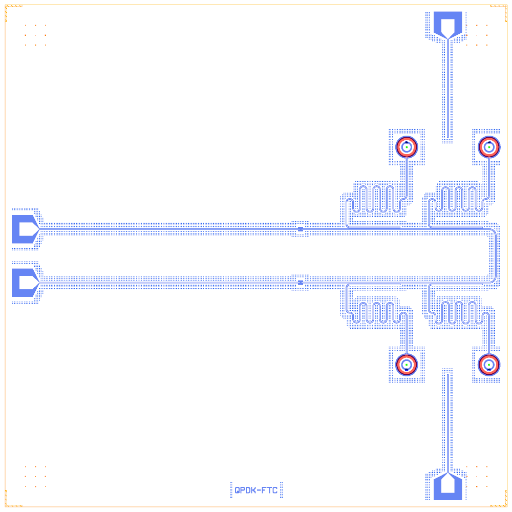
A QPDK test chip with four flipmons: circular flip-chip transmons whose inner disc and outer ring are on the bottom chip, with a disc on the top chip joined by an indium bump. Each flipmon has its own λ/2 readout on a U-shaped probeline. The layout comes from QPDK’s flipmon_test_chip.pic.yml (MIT, after Li et al. 2021) and is rebuilt on the Quantcore PDK; the rebuild is GPL-3.0.
This notebook shows how a two-chip (flip-chip) cell sits in a design: the bottom chip gets the Quantcore frame, the top chip none.
At a glance
Notebook |
|
Source |
gdsfactory |
Chip |
7.5 × 7.5 mm Quantcore die, the source’s 4250 × 6200 µm circuit centred in it, CPW 10 / 6 µm |
On the chip |
4 launchers · 4 flipmons · 4 λ/2 readouts · 1 probeline with 2 series IDCs · 2 flux lines |
Builds today |
yes (layout built on 2026-11-19 in 7 s) |
How the notebook builds it
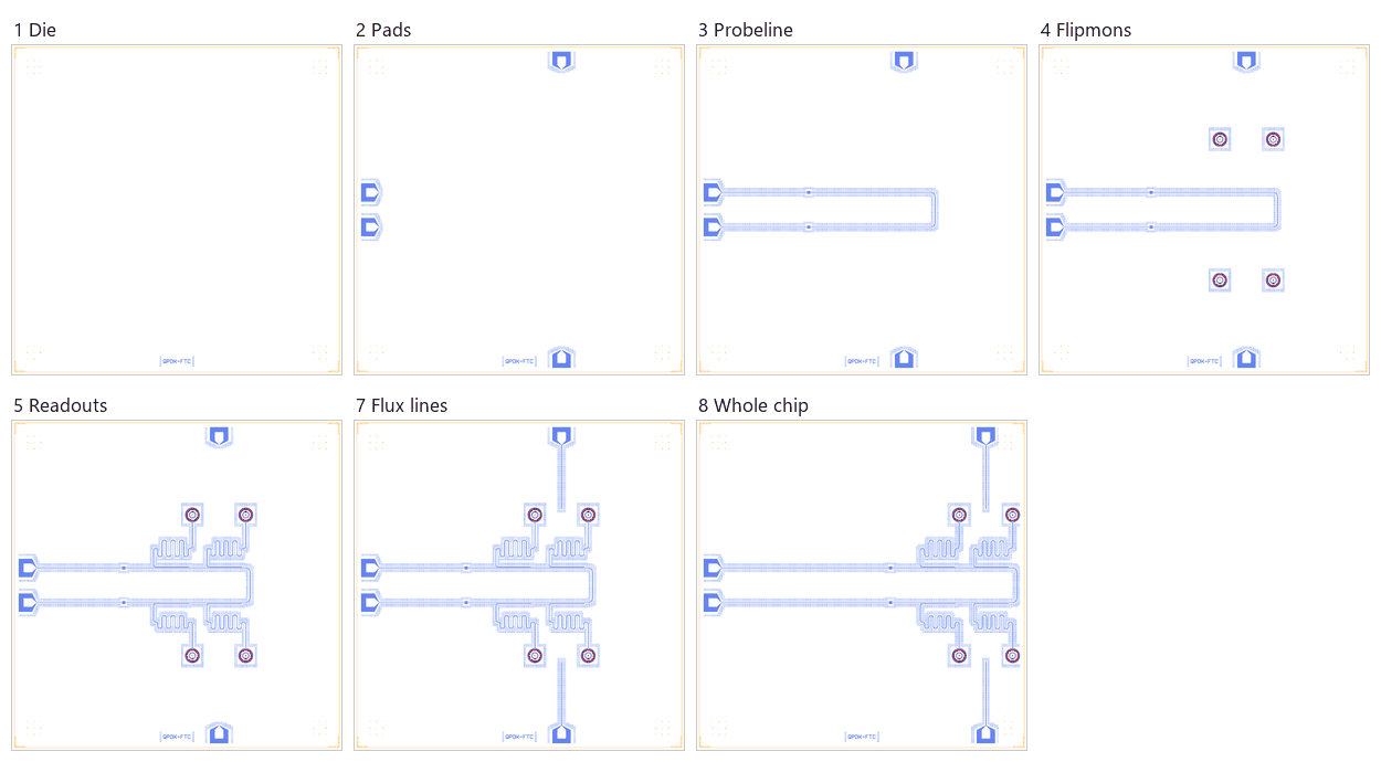
Die. The Quantcore die with the frame and the device ID.
Bond pads. Four launchers, slid to the 100 µm pad-edge rule.
Probeline. The two series IDCs and the U-shaped probeline.
Qubits. Four flipmons, two facing south and two (mirrored) facing north.
Readouts. Four λ/2 readouts from the flipmon plates to coupled sections on the probeline.
Coupling. None.
Flux lines. Two lines from the top and bottom launchers to open ends between the qubit pairs.
Whole chip. Sim groups (one per qubit), the content centred in the die, the design saved.
LOM estimates
Numbers are from a run of this notebook on 2026-11-19 (Setup, Design, Check and the LOM cells, 8 s): QuCat normal modes with QuTiP dressed values.
group |
qubit |
f_q (GHz) |
α (MHz) |
resonator |
f_r (GHz) |
κ (MHz) |
χ (MHz) |
|---|---|---|---|---|---|---|---|
Q1R1 |
Q1 |
5.385 |
-170 |
R1 |
12.35 |
0.748 |
-0.0434 |
Q2R2 |
Q2 |
5.385 |
-170 |
R2 |
12.85 |
0.841 |
-0.0425 |
Q3R3 |
Q3 |
5.385 |
-170 |
R3 |
13.4 |
0.95 |
-0.042 |
Q4R4 |
Q4 |
5.385 |
-170 |
R4 |
13.99 |
1.08 |
-0.0429 |
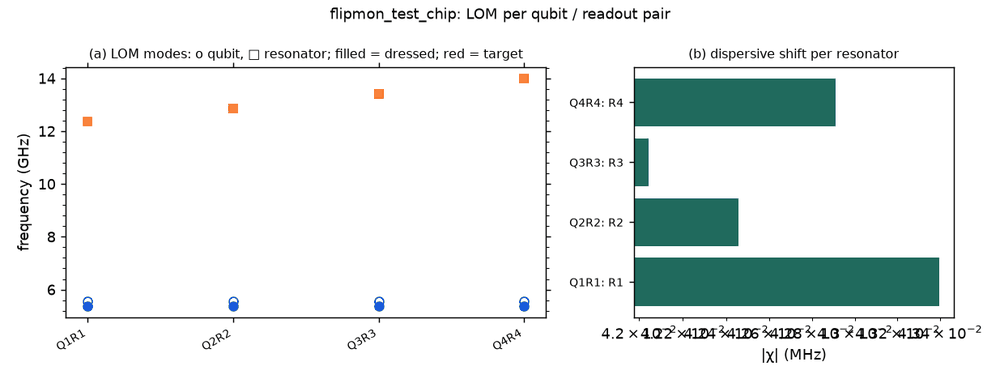
These are lumped-model estimates (component formulas and calibration), not FEM results. The LOM page says how far to trust them.
Build spec
The rest of this page is the detailed spec the notebook was built from, with every component, port, route and length.
Source: qpdk/samples/flipmon_test_chip.pic.yml
(+ flipmon_test_chip.py loader; filled_flipmon_test_chip in filled_test_chip.py) · licence MIT (verified) ·
Read on 2026-11-02. Reference: Li et al. 2021, vacuum-gap transmon qubits (cited as liVacuumgapTransmonQubits2021).
What it is: the qubit test chip netlist line for line. The only changes are the qubit cell
(flipmon_with_resonator_and_probeline) and the resonator lengths; all coupling lengths are the auto default.
The flipmon is a circular transmon. Its inner disc and outer ring are on the bottom chip (M1), with a 110 µm-radius
disc on the top chip (M2) joined through a 15 µm indium bump. Image: docs/_static/images/flipmon_test_chip.png (filled version).
Frame: same as qubit_test_chip: box (0, 0, 4250, 6200), Designer = source + (100, 3100).
The filled version adds an M2 chip edge and fill on the top chip as well.
The first version used the planar KQC ConcentricTransmon as a stand-in (geometry only, no LOM model); the rebuild below uses Flipmon.
Components
Pads, capacitors and flux lines are identical to qubit_test_chip (PAD_IN, PAD_OUT, PAD_FT, PAD_FB, C_IN, C_OUT). Qubits:
instance |
catalog ref |
key params (units) |
at (x, y) Designer |
rot |
notes |
|---|---|---|---|---|---|
Q1 |
|
inner_circle_radius 60, outer_ring_radius 110, outer_ring_width 60, top_circle_radius 110 (M2), bump_diameter 15, m1_etch_extension_gap 30, m2_etch_extension_gap 40, junction |
(2485, 4725) |
coupler faces south |
stand-in: r_inner 60, r_outer 110, outer_island_width 60, ground_gap 30 |
Q2 |
same |
same |
(3715, 4725) |
south |
|
Q3 |
same |
same |
(3715, 1472.6) |
north (mirrored) |
|
Q4 |
same |
same |
(2485, 1471.6) |
north (mirrored) |
Coupler: plate_capacitor_single(width=10, length=58) placed 10 µm outside the outer ring (outer_ring_outside port),
qubit rotated −90°. No Lj is given; assume junction={"Lj_nH": 12, "Cj_fF": 2}.
Routes
FL_IN, FL_OUT, FLUX_T and FLUX_B are as in qubit_test_chip. Every coupler uses the QPDK auto length,
|−900 − x_coupler| − 100 ≈ 800 µm, assuming the plate coupler sits under the qubit centre. The U-turn therefore
moves east. FL: C_IN.b (≈930, 3500) → nodes (3815, 3500), (3815, 2700) → C_OUT.b, with segments [0, 2885] east,
[2885, 3685] south and [3685, 6570] west. Hangers use ground_gap 4 µm, side left. s is the coupler centre.
route |
from → to |
type, length |
hanger (s, length, side, ground_gap, direction) |
coupler x |
|---|---|---|---|---|
R1 |
Q1 coupler → FL.hanger |
meander 5000 |
1055, 800, left, 4, backward |
1585…2385 |
R2 |
Q2 coupler → FL.hanger |
meander 4800 |
2285, 800, left, 4, backward |
2815…3615 |
R3 |
Q3 coupler → FL.hanger |
meander 4600 |
4285, 800, left, 4, forward |
3615…2815 |
R4 |
Q4 coupler → FL.hanger |
meander 4400 |
5515, 800, left, 4, forward |
2385…1585 |
Launchers, pads, test structures, markers, labels
4 launchers. Filled variant: M1 and M2 chip edges plus fill on both faces (M2 fill 80 µm keep-out around M2 metal).
LOM node structure
Q_i: one island node (inner disc + top-chip disc through the bump, in parallel) against the outer ring/ground, with a SQUID. The outer ring is the second electrode, so this is a floating two-node model. The plate coupler gives C_g to R_i.
R_i ↔ FL as in qubit_test_chip. FLUX_T / FLUX_B are flux-bias controls. No bus.
Targets
None stated. As λ/4 on Si, 5000 / 4800 / 4600 / 4400 µm give about 6.0 / 6.2 / 6.5 / 6.8 GHz.
Simplifications for a first rebuild
Planar only:
ConcentricTransmonwithout the top-chip disc and bump. This is a geometry stand-in.The flipmon component: the circular two-face transmon above (M1 disc + ring, M2 disc, bump), with ports
coupler(outer ring) andjunction. It needs multi-face support (KQC faces1t1/2b1).
First build
The first version of examples/designs/qpdk/flipmon_test_chip.ipynb used KQC ConcentricTransmon (r_inner 60, ring 110–170, gap 30, one 18° arc coupler at r 185) as a planar stand-in; top-chip disc and bump not drawn. Readouts λ/2 (open hangers), as in qubit_test_chip. Lj 12 nH assumed.
Rebuild with Flipmon
The ConcentricTransmon stand-in is replaced by Flipmon (QPDK defaults, junction_position_rotation=180; rot 270
for Q1/Q2 = QPDK qubit_rotation=-90, rot 90 for the mirrored Q3/Q4). The QPDK ring is 80–140 µm (ring radius 110 =
centre), not 110–170 µm as listed above. Readouts start at the coupler port, 13 µm beyond QPDK’s plate o1, so
route = resonator_length − 13 µm (4987 / 4787 / 4587 / 4387 µm). LOM (lom Flipmon model, top disc across an assumed
8 µm flip-chip gap, rough; Lj 12 nH assumed): f_q 4.21 GHz, α −197 MHz (was 5.92 GHz / −431 MHz with the planar
stand-in), λ/2 12.55–14.22 GHz, χ −0.03 MHz. Open issue: the Q3D export merges disc and ring into one net (the junction port
finds no edge) and has no 2b1 face.
Quantcore PDK rebuild
The notebook is a Quantcore PDK rebuild, not a replica: the netlist, LOM and imported components are kept, the process is Quantcore’s.
Notebook: examples/designs/qpdk/flipmon_test_chip.ipynb.
Chip: the Quantcore die frame (L dicing markers 1000/0, 3 × 3 alignment grids 1001/0, chip boundary 100/0, device ID where an edge is free; any brand text is QCT), on the 7.5 × 7.5 mm Quantcore die; the source’s 4.25 × 6.2 mm chip area is centred in it (
box=QP.die_box(4250, 6200)), so every coordinate stays the source’s; the top chip (face 2b1) gets no frame (PDK v3 defines none for the flip-chip top chip).Stack: sapphire 650 µm, εr 10.25 (the PDK default stack, used by the LOM estimates and every FEM export); QPDK’s process is Al on Si (εr 11.45), so frequencies are not the QPDK ones.
Junctions: Quantcore trilayer SQUIDs on the PDK rule: two 0.25 × 0.6 µm junctions → R_n 45 kΩ in parallel, L_J 6.73 nH at zero flux, C_J 15 fF; fingers on 2/0 + 4/0, spacer 50/0 with the 51–53/0 gradient (Nb Δ = 1.4 meV, R_n·A 13.5 kΩ·µm² and C_J 50 fF/µm² assumed), radially across the disc–ring gap (
Flipmonjunction_params), in place of the assumed 12 nH + 2 fF. Expected f_q ≈ 5.4 GHz (an estimate; the 12 nH stand-in gave 4.21 GHz).Kept: the topology and every component with the source’s parameters and positions, the readout / resonator lengths and coupled sections, the sim groups (readouts 5000 / 4800 / 4600 / 4400 µm, the 800 µm coupled sections, the assumed 8 µm flip-chip gap).