Qubit test chip (QPDK)
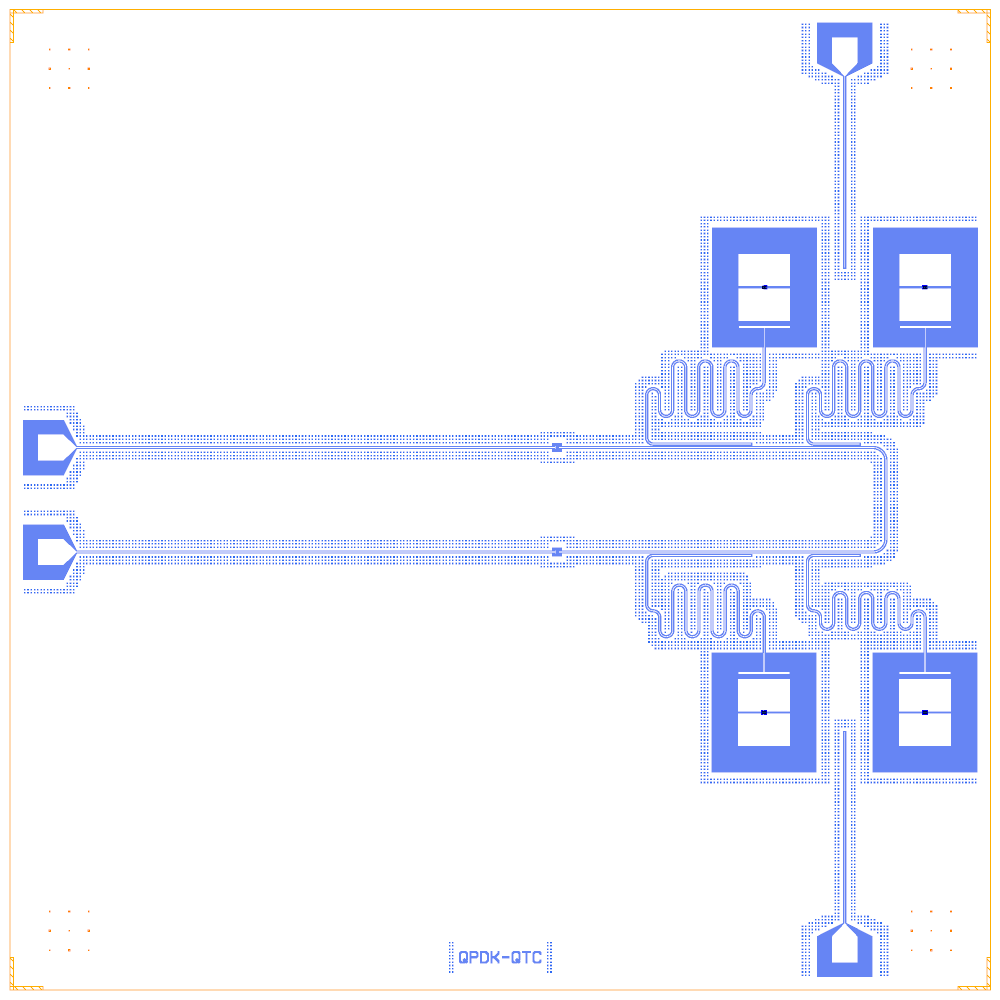
Four floating double-pad transmons, each with a meandered λ/2 readout coupled to one U-shaped probeline, two series IDCs at the probeline ends and two flux lines. The layout comes from QPDK’s qubit_test_chip.pic.yml (MIT, © 2024 gdsfactory) and is rebuilt on the Quantcore PDK: sapphire, trilayer SQUIDs, the QCT die frame. The rebuild is GPL-3.0.
This notebook is an example of a probeline with hanger readouts, the PDK pad rule (launchers 100 µm from the die edge) and the centring of the whole layout in the die.
At a glance
Notebook |
|
Source |
gdsfactory |
Chip |
7.5 × 7.5 mm Quantcore die, the source’s 4250 × 6200 µm circuit centred in it, CPW 10 / 6 µm |
On the chip |
4 launchers · 4 double-pad transmons · 4 λ/2 readouts · 1 probeline with 2 series IDCs · 2 flux lines |
Builds today |
yes (layout built on 2026-11-19 in 7 s) |
How the notebook builds it
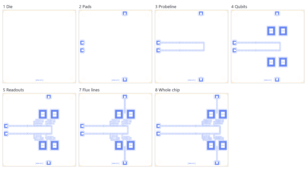
Die. The 7.5 mm Quantcore die with the frame and the device ID.
Bond pads. Four launchers on the 100 µm pad rule.
Probeline. The two series IDCs and the U-shaped probeline.
Qubits. Four
DoublePadstransmons with QPDK’s geometry, Q3 and Q4 mirrored.Readouts. Four λ/2 readouts hanging on the probeline.
Coupling. None: the qubits do not couple to each other.
Flux lines. Two flux lines ending in a 6 µm open gap between the qubit pairs.
Whole chip. Sim groups (one per qubit), the centring (+1660 µm in x), save.
LOM estimates
Numbers are from a run of this notebook on 2026-11-19 (Setup, Design, Check and the LOM cells, 8 s): QuCat normal modes with QuTiP dressed values.
group |
qubit |
f_q (GHz) |
α (MHz) |
resonator |
f_r (GHz) |
κ (MHz) |
χ (MHz) |
|---|---|---|---|---|---|---|---|
Q1R1 |
Q1 |
5.763 |
-196 |
R1 |
11.87 |
0.638 |
-1.36 |
Q2R2 |
Q2 |
5.763 |
-197 |
R2 |
12.86 |
0.206 |
-1.27 |
Q3R3 |
Q3 |
5.764 |
-197 |
R3 |
16.16 |
0.4 |
1.61 |
Q4R4 |
Q4 |
5.763 |
-197 |
R4 |
12.33 |
0.713 |
-1.31 |
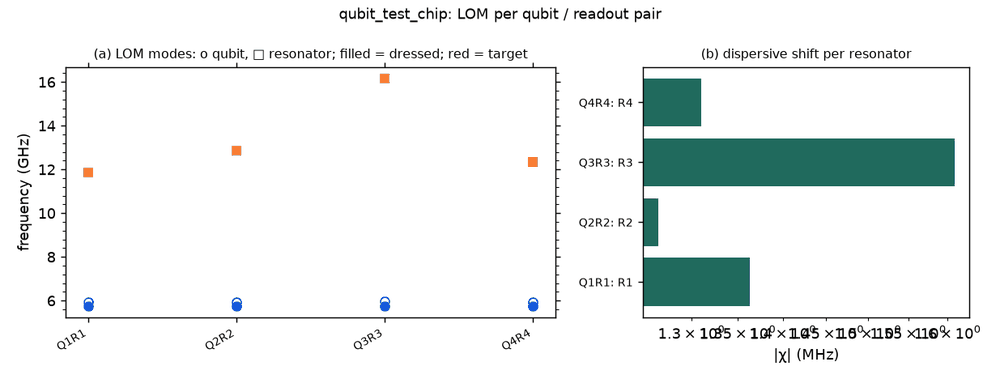
These are lumped-model estimates (component formulas and calibration), not FEM results. The LOM page says how far to trust them.
Build spec
The rest of this page is the detailed spec the notebook was built from, with every component, port, route and length.
Source: qpdk/samples/qubit_test_chip.pic.yml
(gdsfactory YAML netlist; qubit_test_chip.py only loads it) · licence MIT (“Copyright (c) 2024 gdsfactory”, checked
in LICENSE) · Read on 2026-11-02 from a depth-1 clone.
What it is: 4 floating double-pad transmons, each with its own meandered readout line coupled to one probeline that
runs east along y = +400, turns, and runs back west along y = −400 (source frame). Two series interdigital capacitors
at the probeline input and output, two T-shaped flux lines, four launchers. Image: docs/_static/images/qubit_test_chip.png.
Frame: the source has no chip edge. Its extent is x 0…4015, y −3000…+3000 (launchers included). We use the chip edge
of the filled variant (see filled_qubit_test_chip): box (0, 0, 4250, 6200), so
Designer = source + (100, 3100). Layers: QPDK M1_DRAW / M1_ETCH (negative etch), Si εr 11.45.
CPW everywhere: centre 10 µm, gap 6 µm, bend radius 100 µm (cpw). Launcher CPW 200/110 µm.
Every ref resolves (DoublePads, FingerCapacitorSquare, BondPad), and DoublePads has a lumped LOM model.
Components
instance |
catalog ref |
key params (units) |
at (x, y) Designer |
rot |
notes |
|---|---|---|---|---|---|
PAD_IN |
|
default 400×450 pad; QPDK launcher is 200×200 + 100 taper |
(100, 3500) |
270 (port faces east) |
source launcher_in (0, 400); port a ≈ (400, 3500) |
PAD_OUT |
|
same |
(100, 2700) |
270 |
source launcher_out (0, −400) |
PAD_FT |
|
same |
(3100, 6100) |
180 (faces south) |
source launcher_top (3000, 3000) rot −90; flux top |
PAD_FB |
|
same |
(3100, 100) |
0 (faces north) |
source launcher_bot (3000, −3000) rot 90; flux bottom |
C_IN |
|
finger_number 4, finger_length 20, finger_gap 2, finger_width 5 |
(900, 3500) |
0 |
series input capacitor (QPDK |
C_OUT |
|
same |
(900, 2700) |
0 |
series output capacitor |
Q1 |
|
island1/2_extent [400, 250], island_island_gap 15, island_r 0, ground_gap [800, 915], coupler_extent [394, 20], coupler_offset ≈35 |
(2485, 4725) |
180 (coupler faces south) |
source (2385, 1625); QPDK pads 250×400 rotated 90°, 200 µm etched pocket margin |
Q2 |
|
same |
(3715, 4725) |
180 |
source (3615, 1625) |
Q3 |
|
same |
(3715, 1472.6) |
0 (coupler faces north) |
source (3615, −1627.421), mirrored about x |
Q4 |
|
same |
(2485, 1471.6) |
0 |
source (2385, −1628.351), mirrored |
Junction: QPDK squid_junction (2 junctions, loop area 4 µm²). No Lj is stated; use junction={"Lj_nH": 11, "Cj_fF": 2}.
That value is assumed and gives about 5 GHz with C_Σ ≈ 80 fF. The QPDK coupler is a 394×20 µm plate
(plate_capacitor_single) about 45 µm from the pad edge.
Routes
The feedline is a polyline. Hanger s is the coupler centre arclength from FL’s start (C_IN.b ≈ (930, 3500)),
segments [0, 2485] east, [2485, 3285] south, [3285, 5770] west. Probeline ↔ resonator: QPDK coupler_straight
gap 16 µm edge-to-edge, so centre spacing 26 µm and ground_gap = 26 − 5 − 6 − 5 − 6 = 4 µm.
route |
from → to |
type, length |
waypoints / hanger |
notes |
|---|---|---|---|---|
FL_IN |
PAD_IN.a → C_IN.a |
cpw |
straight, y 3500 |
|
FL |
C_IN.b → C_OUT.b |
cpw |
nodes (3415, 3500), (3415, 2700) |
U-turn of |
FL_OUT |
C_OUT.a → PAD_OUT.a |
cpw |
straight, y 2700 |
|
R1 |
Q1.cplr → FL.hanger |
meander 5000 |
s 1055, length 800, side left, ground_gap 4, direction backward |
coupler x 1585…2385 |
R2 |
Q2.cplr → FL.hanger |
meander 4600 |
s 2085, length 400, left, 4, backward |
x 2815…3215; source resonator_meanders 3 |
R3 |
Q3.cplr → FL.hanger |
meander 3600 |
s 3685, length 400, left, 4, forward |
x 3215…2815 on the west-bound leg |
R4 |
Q4.cplr → FL.hanger |
meander 4800 |
s 4715, length 800, left, 4, forward |
x 2385…1585 |
FLUX_T |
PAD_FT.a → free_end((3100, 4875), dir 90, term 6) |
cpw |
straight down x 3100 |
ends in a QPDK |
FLUX_B |
PAD_FB.a → free_end((3100, 1325), dir 270, term 6) |
cpw |
straight up x 3100 |
same tee between Q3 and Q4 |
side="left" is correct on both legs. Going east the resonators lie at +y; going west they lie at −y, which is also
left. In QPDK the resonator line drops from the qubit to the coupler end nearest the qubit, runs along the probeline,
then meanders away from it to an etched open end. The QPDK cell is a resonator_quarter_wave stitched to a coupler
that is open at the qubit plate, so both ends are electrically open. The first spec used the standard λ/4 hanger (short at
the coupler end) with the same total lengths; the notebook uses open λ/2 hangers (see Build below).
Launchers, pads, test structures, markers, labels
4 launchers only. No markers or labels. The filled variant adds the chip edge and vortex fill.
LOM node structure
Q_i: two floating pad nodes, a SQUID between them, C_pad–pad, C_pad–gnd; the coupler plate gives C_g to R_i’s open end.
R_i: CPW resonator (5000 / 4600 / 3600 / 4800 µm) coupled to FL by a 800/400/400/800 µm coupled-line section (4 µm ground strip).
FL: one conductor, PAD_IN → C_IN (series C) → … → C_OUT (series C) → PAD_OUT, two 50 Ω ports.
FLUX_T / FLUX_B: flux-bias controls. Each tee lies between two qubits and shares mutual inductance with both SQUIDs (weak, ~600 µm away).
No qubit–qubit bus.
Targets
None stated in the YAML. As λ/4 on Si (ε_eff ≈ 6.2) the lengths give about 6.0 / 6.5 / 8.3 / 6.2 GHz for R1–R4.
Simplifications for a first rebuild
Drop C_IN/C_OUT and route FL straight from PAD_IN.a to PAD_OUT.a through the same nodes. Subtract ~30 µm from every
s.Flux lines: plain CPW free ends (no tee). KQC
WaveguideCoplanarSplittercan add the tee later.Stand-in qubit: use
Xmon(claw_n toward FL) at the same positions.
Build
The notebook is examples/designs/qpdk/qubit_test_chip.ipynb. The readouts are open hangers (λ/2), not shorted λ/4: QPDK’s line runs from the coupler plate to an etched open end, so both ends are open. Meanders sit between the qubit and the coupled section (r = 50 µm). Launcher ports 110 µm further in (BondPad’s gap runs behind the pad). Lj 11 nH assumed. Flux lines end open (no tee).
Quantcore PDK rebuild
The notebook is a Quantcore PDK rebuild, not a replica: the netlist, LOM and imported components are kept, the process is Quantcore’s.
Notebook: examples/designs/qpdk/qubit_test_chip.ipynb.
Chip: the Quantcore die frame (L dicing markers 1000/0, 3 × 3 alignment grids 1001/0, chip boundary 100/0, device ID where an edge is free; any brand text is QCT), on the 7.5 × 7.5 mm Quantcore die; the source’s 4.25 × 6.2 mm chip area is centred in it (
box=QP.die_box(4250, 6200)), so every coordinate stays the source’s.Stack: sapphire 650 µm, εr 10.25 (the PDK default stack, used by the LOM estimates and every FEM export); QPDK’s process is Al on Si (εr 11.45), so frequencies are not the QPDK ones.
Junctions: Quantcore trilayer SQUIDs on the PDK rule (
_qpdk.JJ_PARAMS): two 0.25 × 0.6 µm junctions (KQC’sjunction_width= the straight finger) → R_n 45 kΩ in parallel, L_J 6.73 nH at zero flux, C_J 15 fF; fingers on 2/0 + 4/0, spacer 50/0 with the 51–53/0 gradient (Nb Δ = 1.4 meV, R_n·A 13.5 kΩ·µm² and C_J 50 fF/µm² assumed), in place of the assumed 11 nH + 2 fF (QPDK states none; its evaporated Al junctions are another process). Expected f_q ≈ 5.8 GHz (an estimate from the earlier LOM C_Σ; the 11 nH junction gave 4.75 GHz).Kept: the topology and every component with the source’s parameters and positions, the readout / resonator lengths and coupled sections, the sim groups (readouts 5000 / 4600 / 3600 / 4800 µm as open-hanger λ/2, coupled 800 / 400 / 400 / 800 µm).