Flip-chip qubit and resonator
A crossmon qubit on the top chip of a flip-chip stack, coupled across a 10 µm gap to the open end of a λ/4 resonator on the bottom chip. It is the Qiskit Metal flip-chip tutorial (Apache-2.0, © IBM and contributors). There are no routes, launchpads or bumps, and the two parts couple vertically. The Quantcore rebuild is distributed under GPL-3.0.
Build this one to learn how a design uses two chip faces at once, how a qubit couples to a resonator through the gap without a route, and how the coupling is declared in the netlist.
At a glance
Notebook |
|
Source |
Qiskit Metal |
Chip |
two faces on the 7.5 mm Quantcore die: control chip (face 1t1) and qubit chip (face 2b1) |
On the chip |
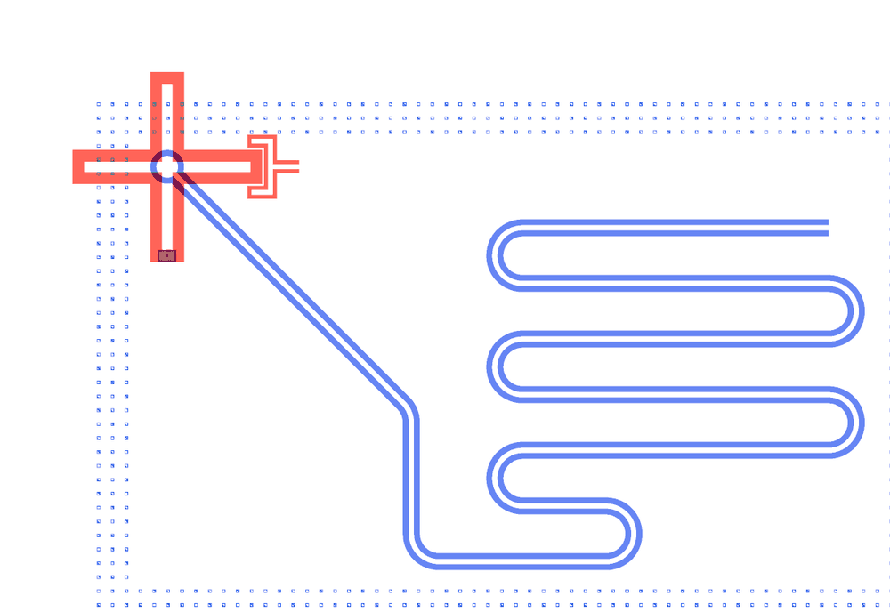
1 crossmon · 1 resonator with a 20 µm disk end under the cross centre · 1 declared vertical coupling |
Builds today |
yes (layout built on 2026-11-19 in 7 s) |
How the notebook builds it
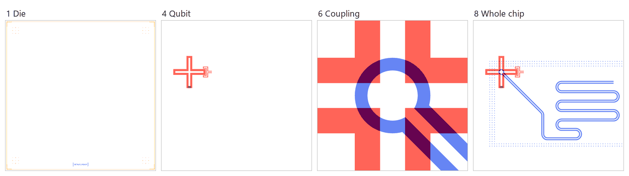
Die. The 7.5 mm die with the QCT frame on face 1t1.
Bond pads. None: the tutorial has no launchpads.
Readout line. None: the resonator is the whole readout.
Qubit. A Metal crossmon on the top chip, with the Quantcore junction.
Readout resonator.
metal:ReadoutResFCon the bottom chip, with a shorted far end.Coupling. The vertical capacitance between the disk and the cross, declared in the netlist.
Control lines. None: the tutorial drives the pair only in HFSS.
Whole chip. The pair centred in the die and the design saved; there is no sim group yet, because the FEM exporter builds one face only.
LOM estimates
Numbers are from a run of this notebook on 2026-11-19 (Setup, Design, Check and the LOM cells, 6 s): QuCat normal modes with QuTiP dressed values.
mode |
kind |
f (GHz) |
κ (MHz) |
A (MHz) |
participation |
|---|---|---|---|---|---|
R1 |
resonator |
6.404 |
0 |
0 |
R1 1.00 |
Q1 |
qubit |
6.788 |
0 |
236 |
J_Q1 1.00 |
group |
qubit |
f_q (GHz) |
α (MHz) |
resonator |
f_r (GHz) |
κ (MHz) |
χ (MHz) |
|---|---|---|---|---|---|---|---|
Q1+R1 |
Q1 |
6.543 |
-269 |
R1 |
6.402 |
0 |
11.6 |
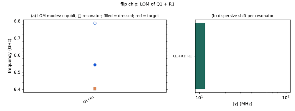
These are lumped-model estimates from component formulas and calibration, not FEM results. The LOM page says how far to trust them.
Build spec
The rest of this page is the detailed spec the notebook was built from: every component, port, route and length.
The
metal:references in this spec build as written, through themetal:wrapper (ports are the Metal pin names, parameters the Metal options). The Quantcore and KQC substitutions are optional. Two faces work through KQCface_ids(top-chip cellsface_ids=["2b1", "1t1", "2t1"], routesd.waypoint(at, face_id="2b1"); seekqc/demo_twoface.md), andmetal:ReadoutResFCbuilds on face 2b1.
The notebook
examples/designs/metal/flipchip_qubit_resonator.ipynbputs Q1 on face 2b1 (face_ids) and R1 on 1t1 and declares the vertical coupling. It has no FEM job yet, because the exporter builds face 1t1 only.
Source: Quantum Metal docs/tut/2-From-components-to-chip/FlipChip-design-tutorial.ipynb. Licence Apache-2.0.
The design uses DesignFlipChip with two facing chips. C_chip (control, bottom, z = 0, extends −280 µm) carries a
ReadoutResFC λ/4 resonator whose open end is a circular pad. Q_chip (qubit, top) carries a TransmonCross whose
east claw sits directly above that pad, so the coupling is vertical across the chip gap. The chips are 10 µm apart:
the notebook changes the default 20 µm, and Q_chip extends +280 µm. The design is analysed by HFSS eigenmode and EPR
(2 modes, Lj 10 nH).
Both chips are 9000 × 9000 µm, centred at (0, 0), so Designer = Metal + (4500, 4500) on each face. Silicon (an
optional custom Si_11.45, εr 11.45, tan δ 1e-7).
The Designer has no face or chip selector for components. The single-face parts map to Xmon and metal:ReadoutResFC.
Components
instance |
face |
catalog ref |
key params (µm) |
at (x, y) |
rot |
notes |
|---|---|---|---|---|---|---|
Q1 |
Q_chip (top) |
|
Metal cross_width 20, cross_length 150 (arm), cross_gap 20; pad |
(4500, 4500) |
0 |
Metal claw pin (4731, 4500) E. Junction on the south arm |
R1 |
C_chip (bottom) |
metal:ReadoutResFC (closest buildable: λ/4 cpw route with an open circular end, not in KQC) |
readout_radius 20, cpw 10/10, turn radius 50, l1 600, l2 200, l3 300, l4 150, l5 550, arc_step 5 |
origin at the pad centre (4500, 4500) |
0 |
footprint x −20…1244, y −715…20 µm relative to the origin; far-end pin |
Routes
None. R1 is drawn as one polygon (l1…l5 plus four 50 µm-radius turns, ≈ 2.1 mm λ/4 centre line). In a two-face
Designer it would be a meander route on the bottom face, from a free_end open pad to a short.
Launchers, pads, test structures, markers, labels
None. There are no launchpads, ports or bumps (flip-chip connectors) in the source.
LOM node structure
Q1 is a cross island with a JJ. The vertical C_g between the Q1 claw and the R1 open pad sits across the 10 µm gap.
R1 is λ/4: open at the pad, with the far end shorted or unconnected (readout pin, short in the simulation). Two
modes (qubit plus resonator). Dielectric loss enters through both chip bulks.
Targets (if stated)
HFSS setup: Lj 10 nH, n_modes 2, min_freq 1.5 GHz, max_delta_f 1 %, max_passes 20. No result values.
Simplifications for a first rebuild
Two single-face sims, e.g. a planar Xmon plus a λ/4 with an open end under the claw, lose the vertical coupling, which is what the tutorial is about.
Wanted: a face parameter on
Designer.add/route(KQC supports faces natively:face_ids, used byDemoTwofaceand theFlipChipConnector*cells). R1 could then be a meander on the bottom face ending in an open pad.
Quantcore PDK rebuild
The notebook is a Quantcore PDK rebuild of the source, not a replica: the netlist, LOM and imported components are kept, and the process is Quantcore’s.
Notebook: examples/designs/metal/flipchip_qubit_resonator.ipynb.
Chip: the Quantcore die frame (L dicing markers 1000/0, 3 × 3 alignment grids 1001/0, chip boundary 100/0, device ID where an edge is free; any brand text is QCT) on the control chip (face 1t1), on the 7.5 × 7.5 mm Quantcore die: the source’s 9 × 9 mm chips hold only the ≈ 1 mm qubit / resonator pair, so the die is centred on them (
box=(750, 750, 8250, 8250), same coordinates). The top (qubit) chip, face 2b1, has no PDK frame (PDK v3 defines none for the flip-chip top chip; its fab layers are 800–804/0).Stack: sapphire 650 µm, εr 10.25 (the PDK default stack, used by the LOM estimates and every FEM export); the source’s custom silicon (εr 11.45) and 10 µm vacuum chip gap are FEM settings; the LOM uses the PDK substrate.
Junctions: Quantcore Nb/AlOx/Nb trilayer junctions (
junction_typefromlayouts.registry.trilayer_junction): fingers on 2/0 + 4/0, spacer 50/0 with the 51–53/0 gradient, sized on the PDK junction rule (Nb Δ = 1.4 meV, I_c·R_n = πΔ/2e, R_n·A 13.5 kΩ·µm² and C_J 50 fF/µm² assumed);Q1gets the PDK nominal junction, 0.5 × 0.6 µm fingers → R_n = 45 kΩ, L_J = 6.73 nH, C_J = 15 fF (in the 40–50 kΩ window), in place of the tutorial’s 10 nH (+ 2 fF assumed); on the top chip its fingers export to the face-2b1 junction layers 803/0 + 804/0 (spacer 50/0). Expected f_q ≈ 6.5 GHz (an estimate), near the 6.49 GHz λ/4.Kept: the topology and every Metal component with the source’s options (through the
metal:wrapper), positions and orientations, every route’s end pins and total length, the sim groups (the two faces, the vertical coupling estimate, the drawn shorted end).