Sixteen junction pads (chip_11f)
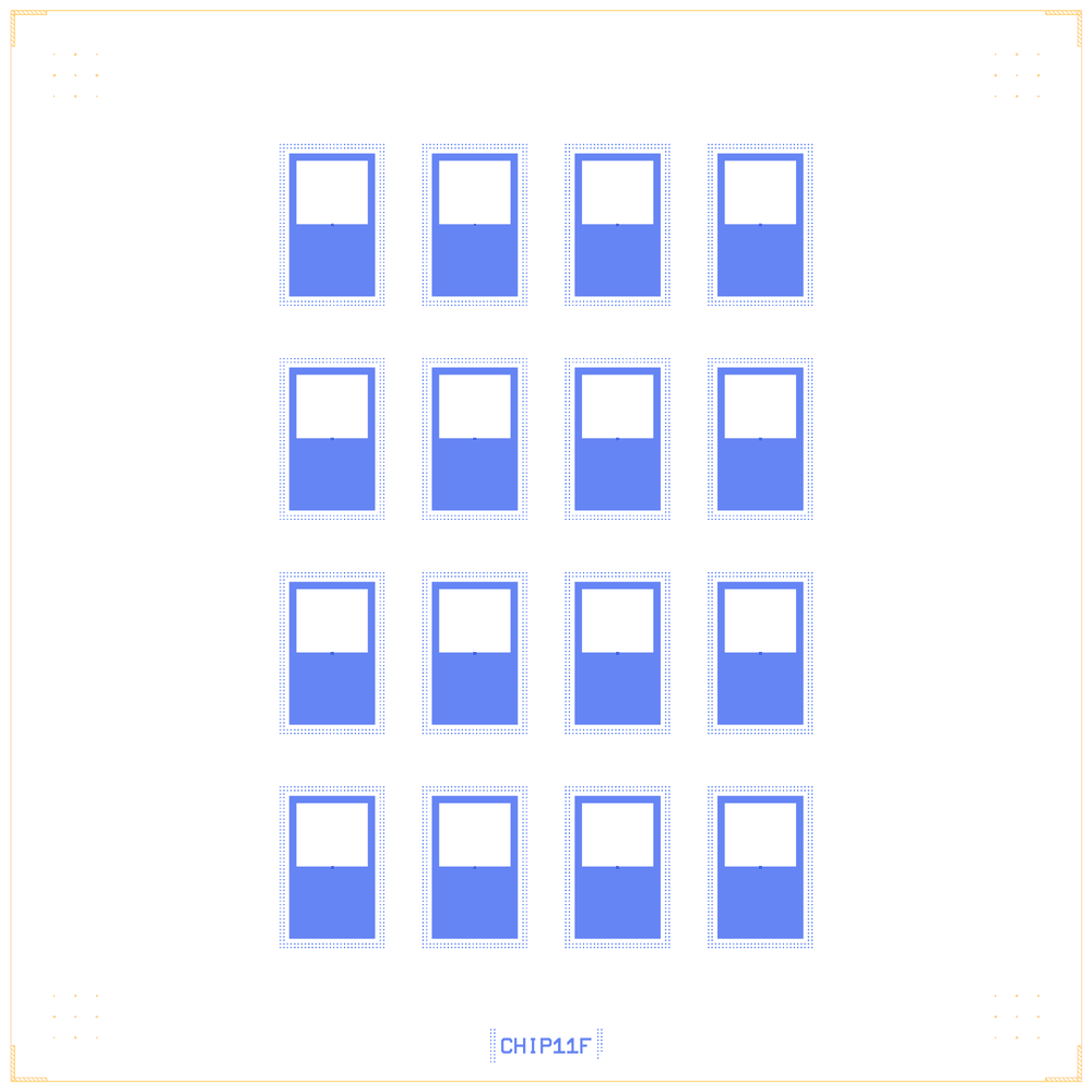
A junction test chip: 16 probe-pad pairs in a 4 × 4 array, each with one small trilayer junction (0.2 × 0.6 µm) in the gap between its two pads. Measuring the resistance across each pair tests how uniform the junctions come out. The legacy script only placed junctions at coordinates read from a CSV file that is now lost, and drew no pads. So the pad pairs, their count and pitch are an assumption: each junction lands in the centre of its pair, overlapping each pad by 1 µm.
It comes from Quantcore’s QWri script chip_11f_JJplacer.py (internal). The rebuild reconstructs a lost layout: it puts the pairs on the PDK die with the PDK cheese band and flags the junctions as higher-resistance than the PDK nominal (112.5 kΩ). Build it to see how a script that only places cells at coordinates becomes a design with explicit sites.
At a glance
Notebook |
|
Source |
Quantcore legacy QWri script |
Chip |
7.5 × 7.5 mm Quantcore die, sapphire |
On the chip |
16 |
Builds today |
yes, rebuilt from its JSON on 2026-11-19 in 0.9 s (the notebook itself was not re-run) |
Pictures
The rebuild: 16 probe-pad pairs in a 4 × 4 array.
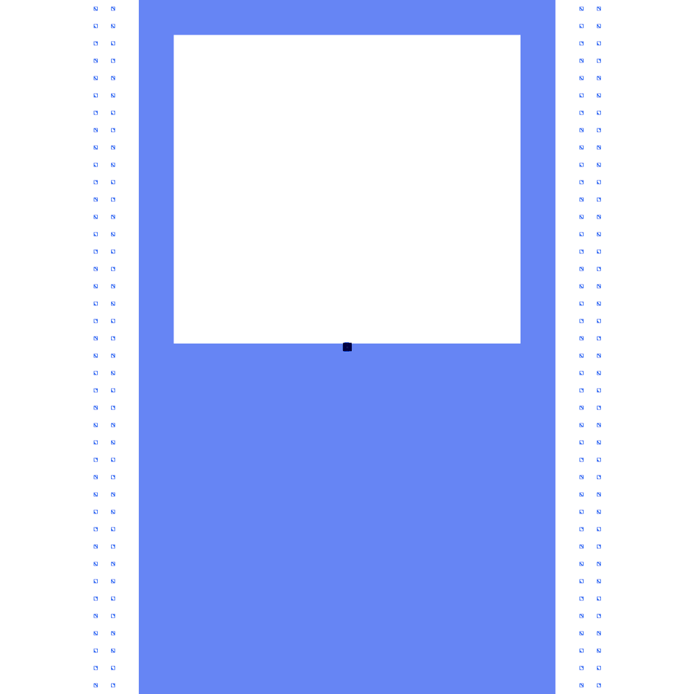
One pad pair, with the junction at the centre where the two pads meet; dots are the cheese band.
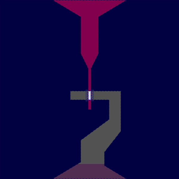
The junction in the gap between the two pad leads (a 20 µm view).
LOM estimates
The notebook has no saved LOM output. The chip has no qubit or resonator, so its LOM netlist is empty.
Build spec
The rest of this page is the detailed spec the notebook was built from: every component, the changes made while rebuilding, and the notes.
Source: components/python/chip_11f_JJplacer.py (module-level script, no function; writes
chip_11m_placed.gds with one cell JJx). Legacy QWri library, Quantcore internal.
Changes made in the rebuild
Built (the coordinates file is lost; the requirement was “the junctions land in the centre of the top and bottom pads, the part that is deleted, with 1 µm overlap”): notebook
examples/designs/legacy/chip_11f_jjplacer.ipynb. 16 pad pairs (4 × 4, pitch 1000 × 1500 µm) of two facingTaperedPads (500 × 350 µm pads, 95 µm taper to 5 µm leads, 600 × 500 µm windows meeting at the pair centre: lead tips at ±5 µm), taken from chip_11m’s commented-out probe pads; one JX_500 (TrilayerJunctionCompact0.2 × 0.6 µm,clearer=True= the legacy centre cut-out) per pair, its 12 µm window centred on the gap so it overlaps each lead by 1 µm. Assumed (to be confirmed): site count / pitch, the lead taper, both pads on M1 (the legacy drew the bottom pad on 3/0). PDK junction rule (Nb trilayer, Δ = 1.4 meV, I_c·R_n = πΔ/2e = 2.20 mV, R_n 40–50 kΩ, qubits 4–8 GHz; PDK processget_pdk().junction: R_n·A 13.5 kΩ·µm², C_J 50 fF/µm², both assumed by the PDK): 112.5 kΩ each.The notebook’s JSON was rebuilt from its layout cell. The notebook has not been re-run, so its outputs are cleared and its PNGs may be out of date.
What it is: a junction-layer placer: it reads x, y, f columns from
D:\Designs\ScriptedDesigns\junctions\jj_coordinates.csv (np.genfromtxt(..., delimiter=',', unpack=True)) and,
for every row, inserts chip_11m’s JX_500 cell (read from chip_11m_jnc1.0_0.6.gds, i.e.
create_testPad(1.0, 0.6): straight finger 0.2 µm, bent finger 0.6 µm) at Trans(f, False, x, y) (rotation
f · 90°, µm). It draws nothing else: no die, no pads, no markers. The output is the junction layers
(2/0, 4/0, HSQ 500/0) of some pre-patterned chip whose pads are not in the library. It also imports
junction_creator_HSQ, squid_creator_HSQ and chip_11m_TestJJ16x_pads without calling them; flip = [1] is
unused.
Reproducing the original: not possible. Every cell resolves (TrilayerJunctionCompact(finger_width=0.2, second_finger_width=0.6)),
but the placement data is missing: jj_coordinates.csv is neither in components/ nor anywhere in the
repository, so the number, positions and rotations of the junctions are unknown. Input needed: the CSV (and, if
it exists, the pad chip it belongs to).
Components (legacy frame)
instance |
legacy cell → catalog ref |
params |
at |
notes |
|---|---|---|---|---|
JX_k (one per CSV row) |
|
as chip_11m, size 1.0 |
|
coordinates from the CSV (missing) |
How it will be built (once the CSV is there)
PDK die frame if the coordinates are on a 7.5 mm die centred on (0, 0) (shift +3750, +3750), else the frame the
pad chip uses; one d.add(f"JX_{k}", "TrilayerJunctionCompact", **L.place(x, y, f), …) per row with the 6 µm origin
offset rotated by f; junction table (one size, L_J ≈ 2.74 nH, R_n ≈ 18.3 kΩ at the assumed Jc = 1 µA/µm²); the
legacy reference through tests/legacy_ref (chip_11m_TestJJ16x_pads.create_testPad(1.0, 0.6) per row) with the
junction-layer XOR (_legacy_b.junction_xor).
LOM
One JJ branch per junction (J_JX_k: JX_k.j to ground); the common ports land on the missing pads. No sim groups.