PDK
The PDK (process design kit, src/quantcore_circuits/pdk/__init__.py) holds the Quantcore fabrication process: the
substrate, the fab layers, the die frame, the keep-outs, the cheese and the junction process. Every build, simulation
export and fab export reads it, so a rule changed here changes every design on the next build. Read this page when a
design must match the fab rules, or when you want to know why the layout puts something where it is.
from quantcore_circuits.pdk import get_pdk
pdk = get_pdk()          # quantcore_nb_sapphire_v1 (default); quantcore_nb_si_v1 is kept for comparison
What it fixes
Item |
Value |
|---|---|
Stack |
Nb film on sapphire 650 µm, eps_r 10.25 (silicon variant: |
Fab layers |
QCT negative mask: 1-4, 50-53, 100, 300 / 301, 700, 800+, 500 / 501 (wafer level), 1000+ |
Die frame |
dicing L, alignment grids, optional device ID, brand |
Pad rule |
the outer edge of a pad’s etch is 100 µm from the die edge |
Keep-outs (3/0) |
route + 10 µm, component + 24 µm, other + 9 µm |
Cheese |
5 µm squares, 20 µm gaps, 4 µm from the 3/0 keep-out, in a band 3 rows wide or ( |
Corner rounding |
on by default in the fab export |
Junction process |
Nb trilayer, R_n 40-50 kOhm per device; cells Quantcore Junction and Quantcore Squid |
Kinetic inductance |
0.116 pH per square; films Nb and NbN ( |
A design names its PDK in design.json (pdk); Designer(pdk=...) does the same. The PDK writes no file of its
own; its rules show up in the layout, in the DRC and in the fab file.
Classes: Pdk, Stack, DieFrame, KeepoutRule, CheeseRule, CornerRounding, JunctionProcess,
KineticInductance. register_pdk adds another PDK.
Tutorial 0 prints the table from the live object with T.pdk_md(pdk).
Pictures
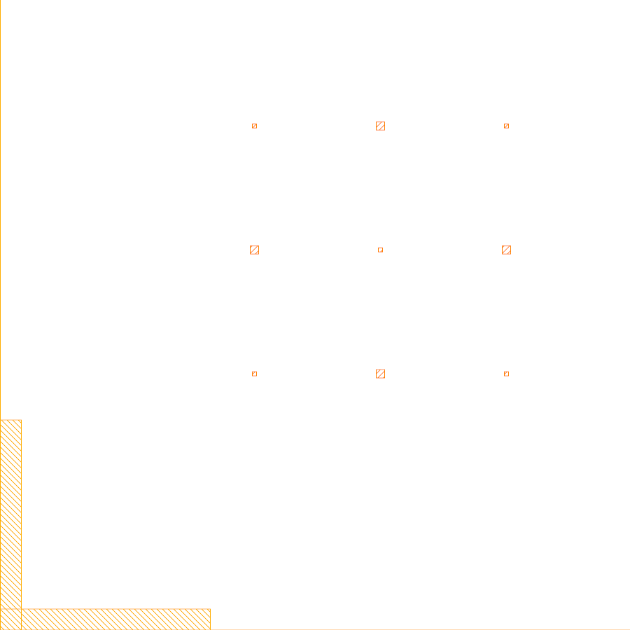
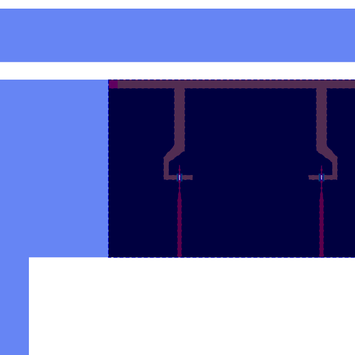
Die frame, lower-left corner: the dicing L and the 3 x 3 alignment grid.
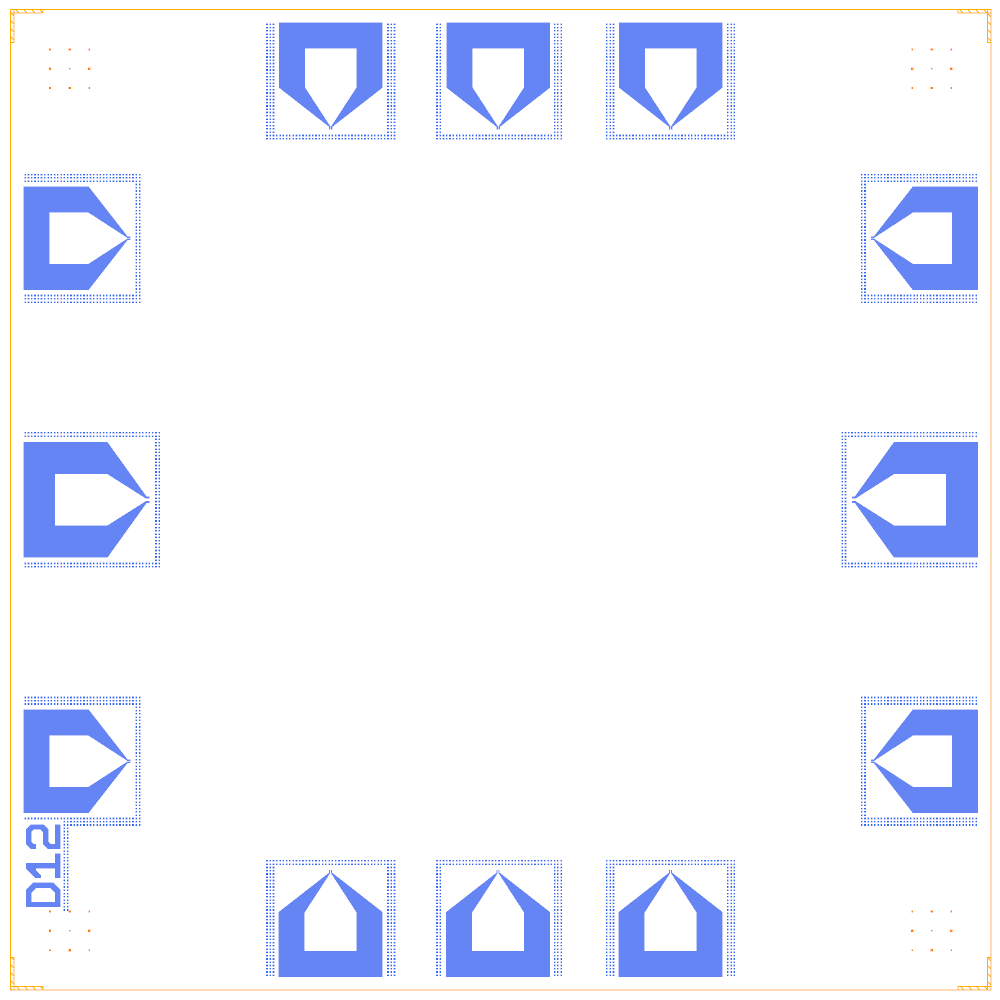
Twelve launchpads of tutorial 1, each placed with edge="auto" so its etch edge is 100 µm from the die edge. The
device ID D12 sits at the lower left.
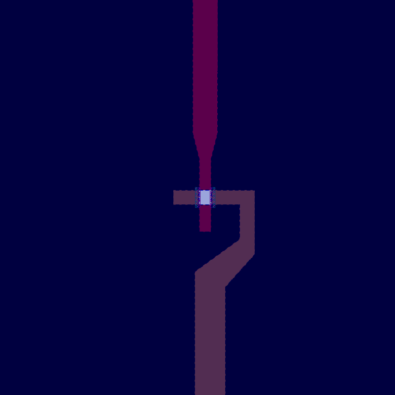
A trilayer junction on the Xmon: lead layers and the junction sheet in the gap of the island.
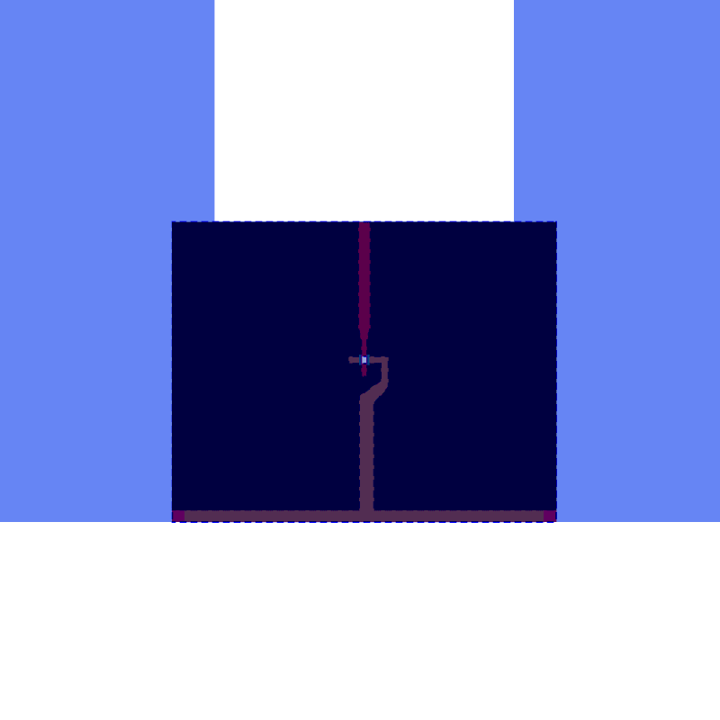
The same junction zoomed to the leads (800 x 800 px render around Q1).
A SQUID: two trilayer junctions in parallel (tutorial 1).
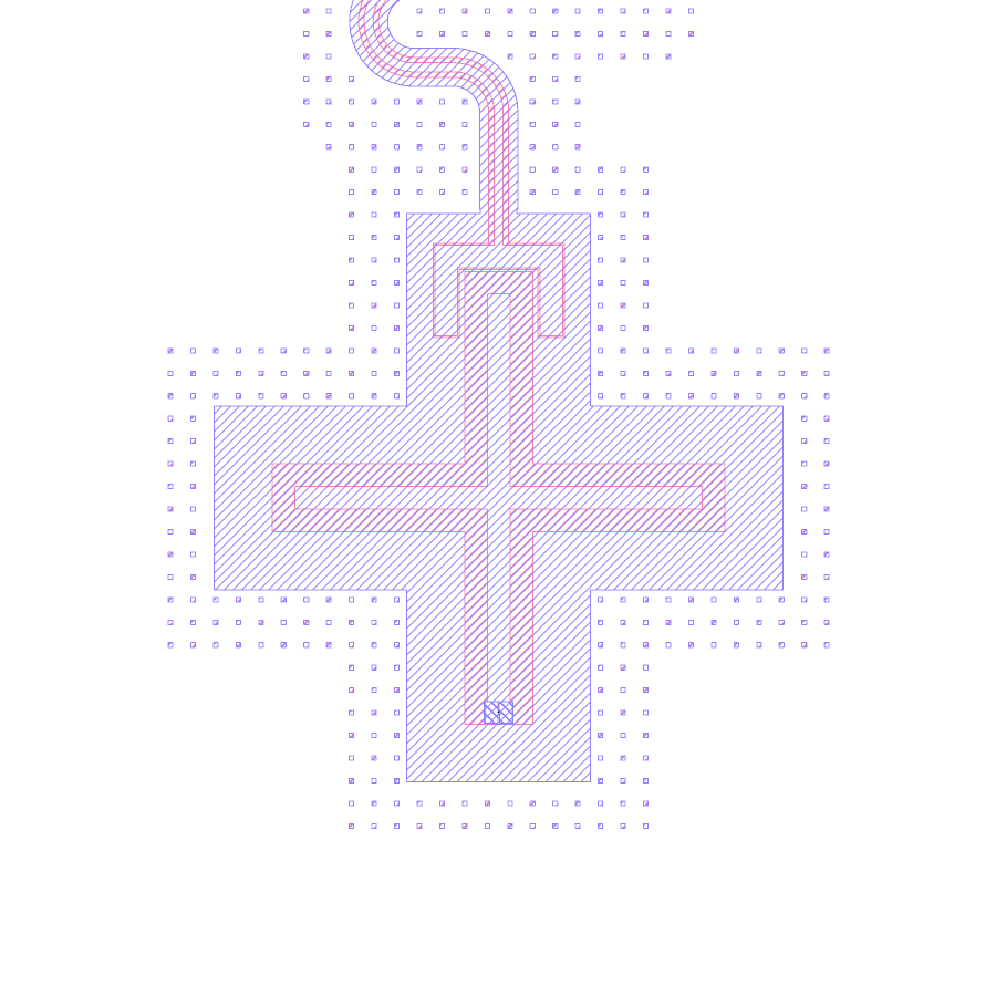
Fab view of a qubit: the metal etch, the 3/0 keep-out and the cheese band around it.
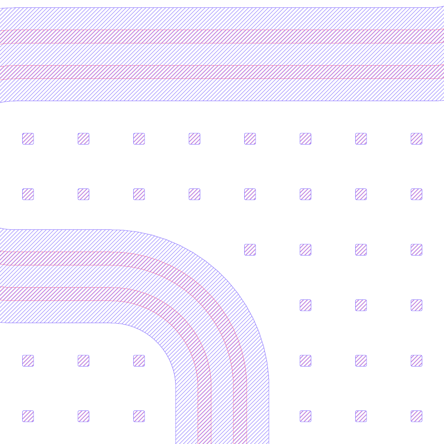
Fab view of a bend: rounded corners and the cheese squares (5 µm squares on a 25 µm pitch).
The rules in practice
Pad rule: bond pads and launchers sit with the outer edge of their etch 100 µm from the die edge.
edge="auto"onDesigner.add(orplace.edgeindesign.json) slides the pad into place.TaperedPadrings count as bond pads for this rule too; aTaperedPadused as a probe pad inside the die gets apad_edgewarning, never an error.Keep-outs (layer 3/0): the metal etch is grown into a keep-out: 10 µm around a route, 24 µm around a component, 9 µm around other shapes. Cells that draw their own keep-out get 4 µm more. A whole KQC chip placed as one instance (such as KQC’s
Stripes,JunctionTestorEmptytest chips), or any cell over more than half the die, counts as other shapes: its etch is grown by 9 µm, not its bounding box by 24 µm, so the ground between its structures stays free for the cheese.Cheese: ground holes (5 µm squares, 20 µm gaps) kept at least 4 µm from 3/0, on 1/0 and on 3/0. By default they fill a band three rows wide around the components. The chip parameter
cheesepicks something else:"chip"spreads the same squares over the whole die (inside the frame, clear of its markers and the device ID; it also switches off a KQCwith_grid),"original"adds nothing, and a dict reproduces an original design’s own rule. A design that already has its own cheese keeps it and gets no band. Holes go in the ground plane only, not in floating pads or islands: metal connected to the die edge, or an isolated piece of at least 1.5 mm² (CheeseRule.ground_island_mm2), which keeps the ground enclosed by a bus ring or a feedline loop. TSVs, indium bumps, under-bump metal and airbridges (pads and flyovers) on the cheese face are kept clear too: no hole within 13 µm of them (the 9 µm margin for other shapes plus the 4 µm clearance), KQC’s automatic ground TSVs and bumps (with_gnd_tsvs,with_gnd_bumps) included. They are not on 3/0, since they sit on the ground metal, and the band is not grown around them. Cheese and corner rounding belong to the fab export only; simulation exports never get them.
Design warnings
Margins against the PDK are DRC warnings of severity design, never errors, and they never block a build or an
export: pad_edge, pdk_rn (junction R_n outside 40-50 kOhm), pdk_fq (qubit frequency outside the band),
pdk_claw. In the plugin, Quantcore > Check > Fix pad edge warnings sets edge = "auto" on every pad the rule flags.
Gaps
The amplifier junction process only has a
pdk_rnwarning.NbN is not selectable per element (only through
Pdk.film).The PDK cheese is drawn on the PDK face (
1t1) only: the top chip (2b1) and the back faces get no holes.Asymmetric SQUID drawn cells and a stored HFSS-versus-Palace bias are not built.
The last rule change made the 3/0 keep-outs 4 µm wider and kept the cheese 4 µm from 3/0; 105 example fab exports were compared after it.