How a design notebook works
Every notebook under examples/designs/ (except legacy/) follows one template, the “v2” form: it builds the chip one
segment at a time with a picture after each, then walks the same steps as the plugin’s Flow strip (Check, LOM,
Simulate, Results, Fab). This page describes the template, the switch cell at the top, the variants, and what to check
on a first run.
On 2026-11-19 every v2 notebook was run up to the whole-chip render (Setup and Design cells), so each one is saved with its layout pictures and its “Same design as before” check. The LOM, Simulate, Results and Fab cells were not run, so run them yourself; the design pages show LOM estimates computed separately. The tutorials are different notebooks, saved with all their outputs.
What a v2 notebook is
The notebook builds the chip the way the chip-12 notebook does, one segment at a time (die, bond pads, readout, qubit placement, coupling, routing, whole chip), so you can see what each step adds. After the layout it follows the plugin’s Flow strip with the same names.
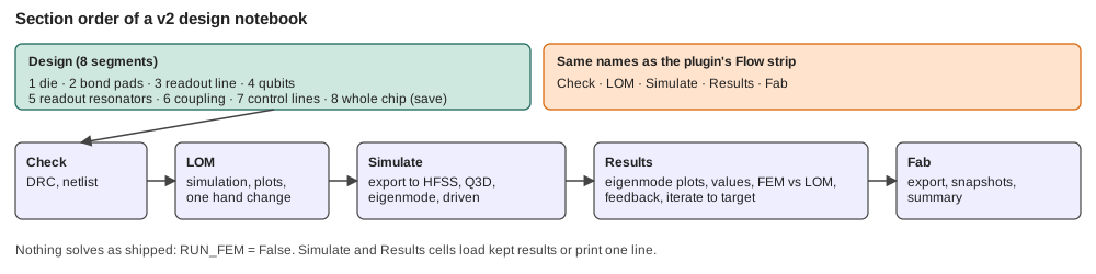
Section order of a v2 design notebook. The headings after Design use the plugin’s step names.
Part |
Cells |
|---|---|
Title, setup, switch cell, PDK table |
the v1 setup is kept; the switches are |
Design 1-8 |
1 die and frame; 2 bond pads ( |
Check |
1 DRC ( |
LOM |
1 simulation ( |
Simulate |
1 export to HFSS ( |
Results |
1 eigenmode plots; 2 the values ( |
Fab |
export, snapshots, summary |
Each Design segment ends with a picture and a line “on the chip so far: n pads, n qubits, …, this step added …”.
Design 8 calls save_design(d, path), which prints “Same design as before” when the saved <id>.json is byte-identical
to the file it replaces. The segmentation only reorganises the same calls with the same arguments, so the JSON does
not change. If it says “differs”, compare with the .v1 notebook and fix the v2.
The same step pictures the v1 notebooks wrote (<id>_step_die.png, _pads.png, _parts.png, _routes.png) show the
progression. These are the ones from metal/a2_two_coupled_transmons (v1 outputs; the v2 adds a picture per segment):
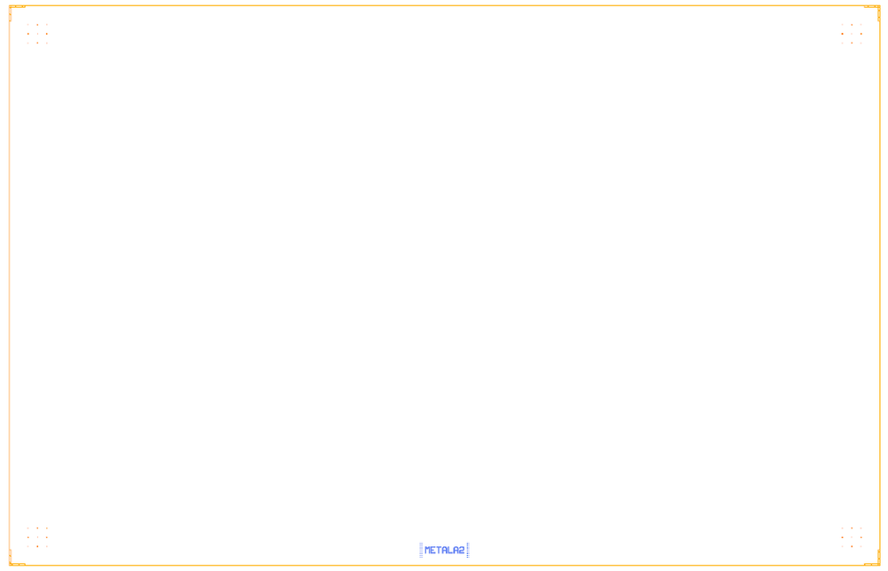
Step 1: the empty die with the PDK frame and the device ID (v1 output of a2_two_coupled_transmons).

Step 2: a bond pad at the 100 µm rule, with the cheese band beside it.
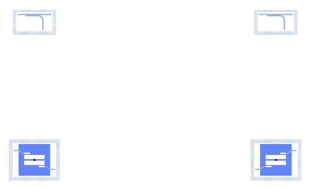
Step 3: the components placed before any route (v1 _step_parts.png).
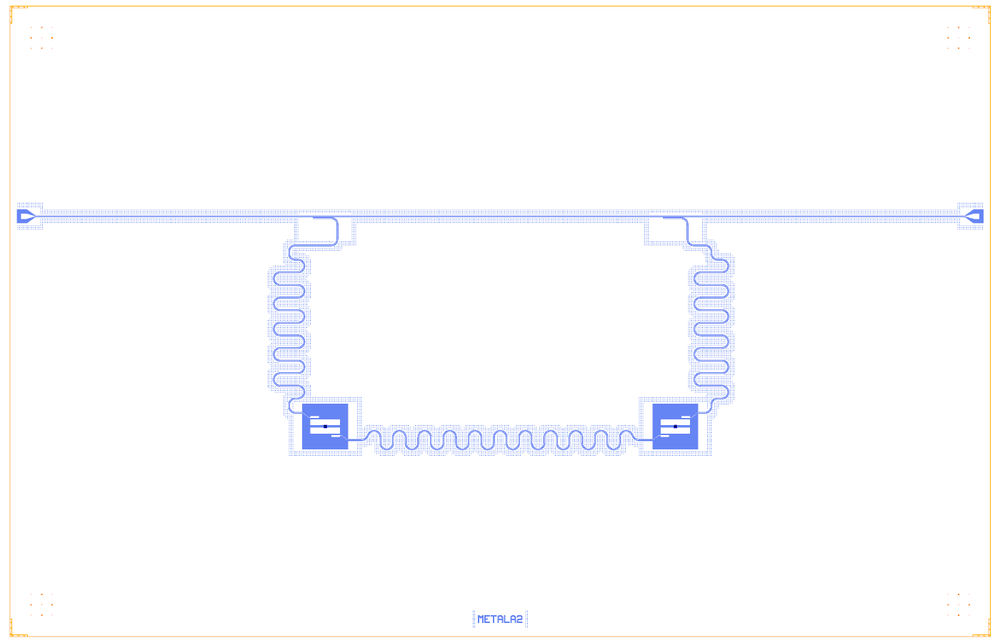
The whole chip with its routes (v1 _step_routes.png).
The switch cell: nothing solves as shipped
Switch |
Meaning |
|---|---|
|
No AEDT is started. Simulate cells export the jobs and print “no solved results yet” unless kept results exist; Results cells load kept results from |
|
Do not solve again when kept results of the same revision exist |
|
Fast solver settings: minutes per solve, not converged |
|
|
|
Revisions tried by the iterate cell |
With RUN_FEM = True (AEDT 2024 R1 or later, FEM_FAST = True) the cells solve and keep results; set it back to False
and the Simulate and Results cells load them. Timings seen on the workstation: Q3D 1-5 min per component box,
eigenmode 2-17 min, driven 3-8 min.
Variants
The template is variant A. The others differ where the chip’s geometry fixes the order or the chip is one PCell.
Variant |
Chips |
What changes |
|---|---|---|
A. Qubit chips |
metal, community, google, ibm, squadds, sqdmetal, qpdk and KQC qubit chips |
The template. No feedline: segment 3 holds the readout pads. No pads: segment 2 says so in one sentence |
B. Amplifiers |
the six |
Die, pads, feed or pump lines, the nonlinear element (JJ chain, KI serpentine, SQUID, KI resonator), routing, whole chip. LOM uses the v1’s own models. Eigenmode and driven runs only where a sim group fits: none for the two TWPAs or |
C. Test chips drawn element by element |
|
Die, launchers, test structures, routing, whole chip. LOM and Simulate only where there is a circuit or a sim group. Results are the XOR against KQC |
D. One-PCell chips |
eight KQC test chips and |
The chip cannot be split without redoing the PCell, so the segments are views: the empty die, the PCell placed with |
E. Plan-driven chips |
|
The segments are the calls of the shared |
F. Order fixed by geometry |
|
The v1 call order is kept where a position depends on an earlier one (centring before the pads, parts placed from a qubit port, snap chains). The headings follow the real order and say why |
G. Derived or gallery |
|
Views of loaded or gallery content; no sim groups are added |
All rewritten notebooks
Group |
Notebooks (variant) |
|---|---|
|
|
|
|
|
|
|
|
|
|
|
|
|
|
|
|
|
|
|
|
|
|
The legacy/ group was not rewritten.
The .v1 notebooks
Beside every rewritten notebook sits <id>.v1.ipynb: a byte copy of the old notebook with its saved outputs, left
unedited. Use it to see what the old run printed (the v2 marks such run values “(from the v1 run)”) or to get the old
one-step layout. A .v1 writes the same <id>.json, build/<id>.oas and step pictures as the v2, so run one or the
other, not both in a row, if you want to compare files. The test suite and scripts/design_status.py know about the
pairing (a v2 without outputs reports the v1’s state).
Checklist for the first run
Run top to bottom, live or with QCC_LIVE=0 and OPENBLAS_NUM_THREADS=2, switches as shipped first.
Each Design segment shows its picture and its “on the chip so far” line; the counts grow segment by segment.
Design 8 prints “Same design as before”, and
git diff examples/designs/<group>/<id>.jsonis empty.The Check and LOM tables equal the
.v1notebook’s saved outputs; the LOM 2 plots appear.Simulate cells print “no solved results yet” and export the jobs; no AEDT starts.
Results 1-3 print their “no results yet” lines. Results 4 runs
loop.analyseandloop.feedback(minutes on 4+ qubits) and gives a proposal, a revision and “DRC: clean”. If it says “no target reached the consensus”, see R3 below.Results 5: the history table ends “on target: yes” within
MAX_ITER(on the LOM) and the residual plot falls below 1.Fab and the snapshots as in the v1.
Then
RUN_FEM = True. Watch: eigenmode boxes that cut a line on a bend (no port polygon; the builder warns), a missing S21 notch on pad-terminated readouts (m51,a5: kappa from the eigenmode Q instead), and pyEPR p_J near 1 on the qubit mode.With kept FEM: Results 3 shows LOM, LOM on the Q3D C-matrix and eigenmode side by side; Results 4 anchors on the FEM point; Results 5 with
RUN_FEM = Truesolves each revision’s component jobs (fem/rev<k>/).
A static checker, python scripts/check_notebook_api.py NB.ipynb [--clean], reads a notebook without running it: schema,
syntax, names, imports and the signatures of every resolvable call.
Known gaps
No mesh reuse (R1). The library cannot reuse a solved eigenmode mesh in a driven setup.
driven_from_eigenmodesubstitutes the same group and box, the eigenmode job’smesh_sizeseeds, the adaptive frequency at the eigenmode’s resonator mode and a fast sweep around it. The cell says so.Feedback only knows qubit-readout pairs.
loop.feedbacktunes pairs; buses, couplers, amplifiers, test structures and qubits without a readout use a notebook-side first-order rule (lambda proportional to 1/f, L_J proportional to 1/f squared). The iterate cell withoutRUN_FEMjudges revisions on the LOM, so a FEM minus LOM offset is not carried on (tutorial 4 does the space mapping by hand).Drawn junction after feedback (R2). The feedback changes
<Q>.junction.Lj_nH; designs that draw the PDK nominal fingers keep drawing them.Several designs carry targets outside the PDK windows, so feedback bounds are the model’s defaults (R8, R11).
The ranked library requests are in status page.