A custom qubit with its junction
This page builds a qubit that is not in the library: a floating transmon whose two islands are forks. It takes one
Python class (examples/custom_component/custom_qubit.py) with the shape, two pins, a Quantcore trilayer junction
across the gap and a LOM model. Afterwards Designer.add, d.route, d.drc() and d.lom() work with it as with any
library qubit. The notebook that runs every step is examples/custom_component/custom_qubits.ipynb.
What we build
Part |
Choice |
|---|---|
Islands |
Two equal islands, a neck (30 µm wide) towards the junction, a body with a slot cut from the outer end (the fork), rounded corners |
Junction |
The PDK trilayer junction across a 20 µm gap between the two necks |
Pin |
A readout claw beside the top island, with a tail that continues as the readout CPW. Direction +x |
Pin |
An open-ended drive stub that ends beside the bottom island. Direction -x |
LOM |
Two islands, C between them, the junction between them, the claw as a node, the drive as a control line |
1 · The class and its parameters
Every number of the shape is a parameter, so the plugin panel and design.json can change it. The two junction
parameters are the ones every Quantcore qubit has: junction_type picks the trilayer cell, junction_params sizes it.
from kqcircuits.elements.element import Element
from kqcircuits.pya_resolver import pya
from kqcircuits.util.parameters import Param, pdt


class ForkTransmon(Element):
    qcc_category = "qubit"      # panel filter, DRC, fab export and LOM read this
    qcc_junction = True

    body_w = Param(pdt.TypeDouble, "Island body width", 240, unit="μm")
    body_len = Param(pdt.TypeDouble, "Island body length", 260, unit="μm")
    neck_w = Param(pdt.TypeDouble, "Neck width (towards the junction)", 30, unit="μm")
    neck_len = Param(pdt.TypeDouble, "Neck length", 40, unit="μm")
    slot_w = Param(pdt.TypeDouble, "Fork slot width (0 = no fork)", 50, unit="μm")
    slot_len = Param(pdt.TypeDouble, "Fork slot depth from the outer end", 130, unit="μm")
    gap = Param(pdt.TypeDouble, "Junction gap between the two necks", 20, unit="μm")
    clearance = Param(pdt.TypeDouble, "Etched clearance around the islands", 40, unit="μm")
    # ... claw_w, claw_len, claw_gap, tail_len, drive_gap, corner_r
    junction_type = Param(pdt.TypeString, "Junction across the gap", "Quantcore Junction",
                          choices=["No Squid", "Quantcore Junction", "Quantcore Squid", "Trilayer Junction",
                                   "Trilayer Squid", "Sim"])
    junction_params = Param(pdt.TypeString, "Trilayer junction cell parameters (JSON dict, e.g. lj_nH)", "{}")
2 · The geometry
build() works in the cell’s own frame, with the junction gap centred on the origin: island 1 below, island 2 above.
Each island is one polygon (neck, body, slot), the corners are rounded with Region.round_corners.
def _island(self, sign):                       # +1 top island, -1 bottom island
    g, nl, bl = self.gap / 2, self.neck_len, self.body_len
    bw, nw = self.body_w, self.neck_w
    y0, y1, y2 = g, g + nl, g + nl + bl        # gap edge, neck/body step, outer end
    hs, sd = self.slot_w / 2, self.slot_len
    pts = [(-nw/2, y0), (nw/2, y0), (nw/2, y1), (bw/2, y1), (bw/2, y2),
           (hs, y2), (hs, y2 - sd), (-hs, y2 - sd), (-hs, y2),      # the fork slot
           (-bw/2, y2), (-bw/2, y1), (-nw/2, y1)]
    return pya.DPolygon([pya.DPoint(x, sign * y) for x, y in pts])
The cell draws a negative mask, so it draws what is removed. The etched pocket is the clearance around the
islands and the claw, plus a CPW gap b along each tail, minus all the metal:
islands = self._round(pya.Region([self._island(1).to_itype(dbu), self._island(-1).to_itype(dbu)]))
metal = islands + claw + tails                                  # claw bar and the two tails
clear = (islands + claw).sized(round(self.clearance / dbu), 2)  # clearance around the islands
etch = (clear + corridors) - metal                              # corridors: gap b beside each tail
self.cell.shapes(self.get_layer("base_metal_gap_wo_grid")).insert(etch)
self.add_protection(pya.Region(etch.bbox()).sized(round(self.margin / dbu)))   # no cheese here
3 · The pins
A pin is a name, a position and the direction that points out of the component. A route leaves or arrives along it.
The tail ends at the pin, and the route continues as a CPW of centre width a and gap b.
self.add_port("claw", pya.DPoint(self._x_claw_port(), yc), pya.DVector(1, 0))
self.add_port("drive", pya.DPoint(self._x_drive_port(), yd), pya.DVector(-1, 0))
4 · The junction
place_trilayer inserts the Quantcore trilayer junction cell across the gap. You give it the two ends of the junction
line: the island side first, the ground side (here the other island) second. It sizes the window to the gap, draws the
fingers on 2/0 and 4/0 (KQC layers SIS_junction and SIS_junction_2), the clearer metal box and the spacer. The two
refpoints port_squid_a / port_squid_b mark the junction ends for the simulation export.
a_pt, b_pt = pya.DPoint(0, self.gap / 2), pya.DPoint(0, -self.gap / 2)
self.refpoints["port_squid_a"], self.refpoints["port_squid_b"] = b_pt, a_pt
if self.junction_type not in ("No Squid", "Sim"):
    from quantcore_circuits.layouts.junctions.trilayer import place_trilayer

    gaps = pya.Region(self.cell.begin_shapes_rec(self.get_layer("base_metal_gap_wo_grid")))
    place_trilayer(self, self.junction_type, gaps, a_pt, b_pt, self.junction_params)
Simulation builds set junction_type to "Sim", so the clearer never shorts a FEM model.
5 · Register it and look at it
A class outside the package registers itself into the KQC library when its module is imported (the last lines of
custom_qubit.py). Put the folder on sys.path and use the dotted path as the cell reference.
import sys
sys.path.insert(0, "examples/custom_component")
from quantcore_circuits.designer import Designer
from quantcore_circuits.layouts.registry import trilayer_junction
from quantcore_circuits.live.snapshot import snapshot

params, junction = trilayer_junction("custom_qubit.ForkTransmon")      # the PDK nominal junction
d = Designer("qc_fork_alone", box=(0, 0, 7500, 7500), live=False)
d.add("Q1", "custom_qubit.ForkTransmon", at=(3750, 3750), junction=junction, **params)
d.show()
snapshot(d.out, "qubit_cell.png", box=(3250, 3300, 4250, 4200))
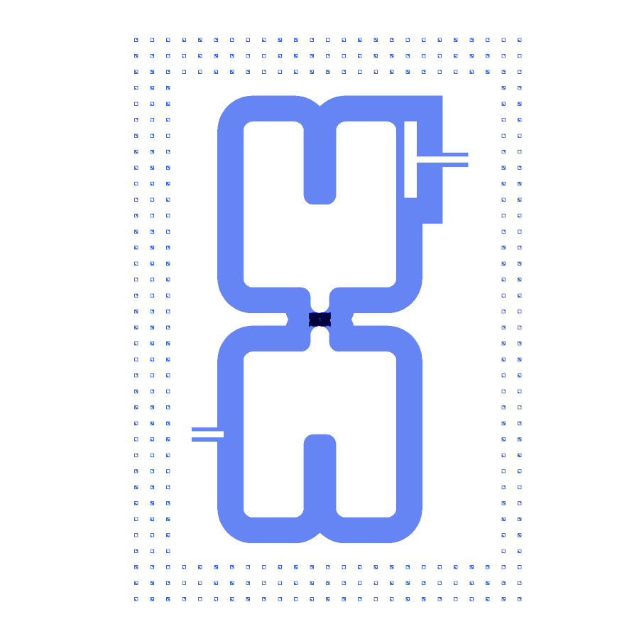
Blue is what is etched. The islands are the white shapes inside the etch, the claw is the bar to the right of the top island and the drive stub is the short line to the left of the bottom island. At the centre is the junction:
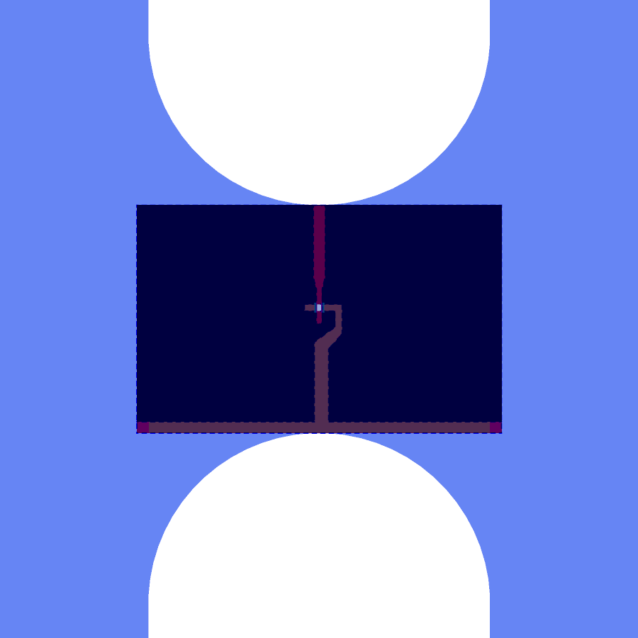
trilayer_junction(cell, lj_nH=...) returns the two things a qubit needs: the cell parameters (junction_type,
junction_params) that make the junction the PDK trilayer junction sized for that L_J, and the drawn junction’s
{"Lj_nH", "Cj_fF"} for the instance’s junction. The L_J comes out slightly different from the one you asked for,
because the fingers sit on the PDK grid.
6 · The LOM model
The model is a qcc_lom class method that returns a Fragment: the nodes of the component, the elements between them
and which pin is which node. The component has no calibration, so the capacitances are formulas from
quantcore_circuits.lom.estimates, marked as "rough".
@classmethod
def qcc_lom(cls, name, inst, pdk):
    p = cell_params(inst)                       # the defaults merged with the instance's parameters
    eps = est.substrate_eps(pdk)
    c_island = est.pad_to_ground(bw, bl, clr, clr, eps) + ...        # body + neck + the slot walls
    c_mut = est.coplanar_coupling(nw, nl, nl, gap, eps) + ...        # the necks facing across the gap
    frag = Fragment(
        nodes={"island1": {"island": f"{name}.island1"}, "island2": {"island": f"{name}.island2"},
               "claw": {"island": f"{name}.claw"}},
        port_nodes={"claw": "claw", "drive": "control:drive", "squid_a": "island1", "squid_b": "island2"},
    )
    frag.elements += [
        LomElement(f"C_{name}_1", "C", ("island1", "gnd"), est.cap(c_island, "rough", formula)),
        LomElement(f"C_{name}_2", "C", ("island2", "gnd"), est.cap(c_island, "rough", formula)),
        LomElement(f"C_{name}_12", "C", ("island1", "island2"), est.cap(c_mut, "rough", formula)),
        # ... Cg_<name>_claw (claw to island 2) and Cc_<name>_claw (claw to ground)
        junction_element(name, "island1", "island2", inst, "JJ", drawn_params=p),    # L_J from the PDK rule
    ]
    return frag
Notes on the model:
"island"names the FEM net of each node (Q1.island1, …). A Q3D C-matrix of the cell fills the capacitances by these names.port_nodessays which node each pin is."control:drive"marks a pin that carries a control line (a drive or flux line), not a circuit connection.junction_elementtakes L_J from the instance’sjunctionif the design gives one, else from the drawn trilayer junction on the PDK rule. It never invents a value.
An alternative to the class method is @register_lom("ForkTransmon") from quantcore_circuits.lom.fragment, as in
pad_gap_capacitor.py. Both work; subclasses inherit the model.
7 · Place it on a chip
The chip is two bond pads, a feedline, the qubit and a λ/4 readout resonator. The first step sizes the junction for
the target: the LOM gives the capacitances, size_junction the L_J and the R_n it implies.
from quantcore_circuits.circuit.bridges import size_junction, tl_resonator
from quantcore_circuits.pdk import get_pdk

pdk = get_pdk()
d = Designer("qc_fork_chip", box=(0, 0, 7500, 7500), chip={"name_chip": "QC1"}, live=False)
pw = d.add("PAD_W", "BondPad", at=(1125, 3750), rot=270, edge="auto")
pe = d.add("PAD_E", "BondPad", at=(6375, 3750), rot=90, edge="auto")
fl = d.route("FL", pw.a, pe.a)

params, junction = trilayer_junction("custom_qubit.ForkTransmon")
q1 = d.add("Q1", "custom_qubit.ForkTransmon", at=(3750, 2300), body_w=300, body_len=300,
           junction=junction, **params)
c = {n: b.value["estimate"] for n, b in d.lom().model.branches.items() if b.type == "C"}
c_sigma = c["C_Q1_1"] * c["C_Q1_2"] / (c["C_Q1_1"] + c["C_Q1_2"]) + c["C_Q1_12"] + c["Cg_Q1_claw"]
s = size_junction(5.5, c_sigma, c_includes_junction=False)          # L_J and R_n for 5.5 GHz
params, junction = trilayer_junction("custom_qubit.ForkTransmon", lj_nH=s.lj_nH)
q1.set(junction=junction, **params)
With the 300 × 300 µm body, C_Σ is about 99 fF, so 5.5 GHz needs L_J = 6.96 nH, R_n = 46.5 kΩ: inside the PDK window of 40-50 kΩ. A smaller body would need a higher R_n, which the DRC reports as a PDK design warning.
The readout is a route from the claw to a hanger on the feedline. Routes start at any pin, so q1.claw works like the
Xmon’s claw_n.
vp = tl_resonator(4500, pdk.cpw_a, pdk.cpw_b)["vp_m_s"]
L_R1 = vp / (4 * 7.0e9) * 1e6                                        # bare λ/4 for 7 GHz (µm)
r1 = d.route("R1", q1.claw, fl.hanger(near=(4400, 3750), length=300, side="right"), meander=L_R1, r=50)
d.targets(Q1={"f_q_GHz": 5.5}, R1={"f_GHz": 7.0})
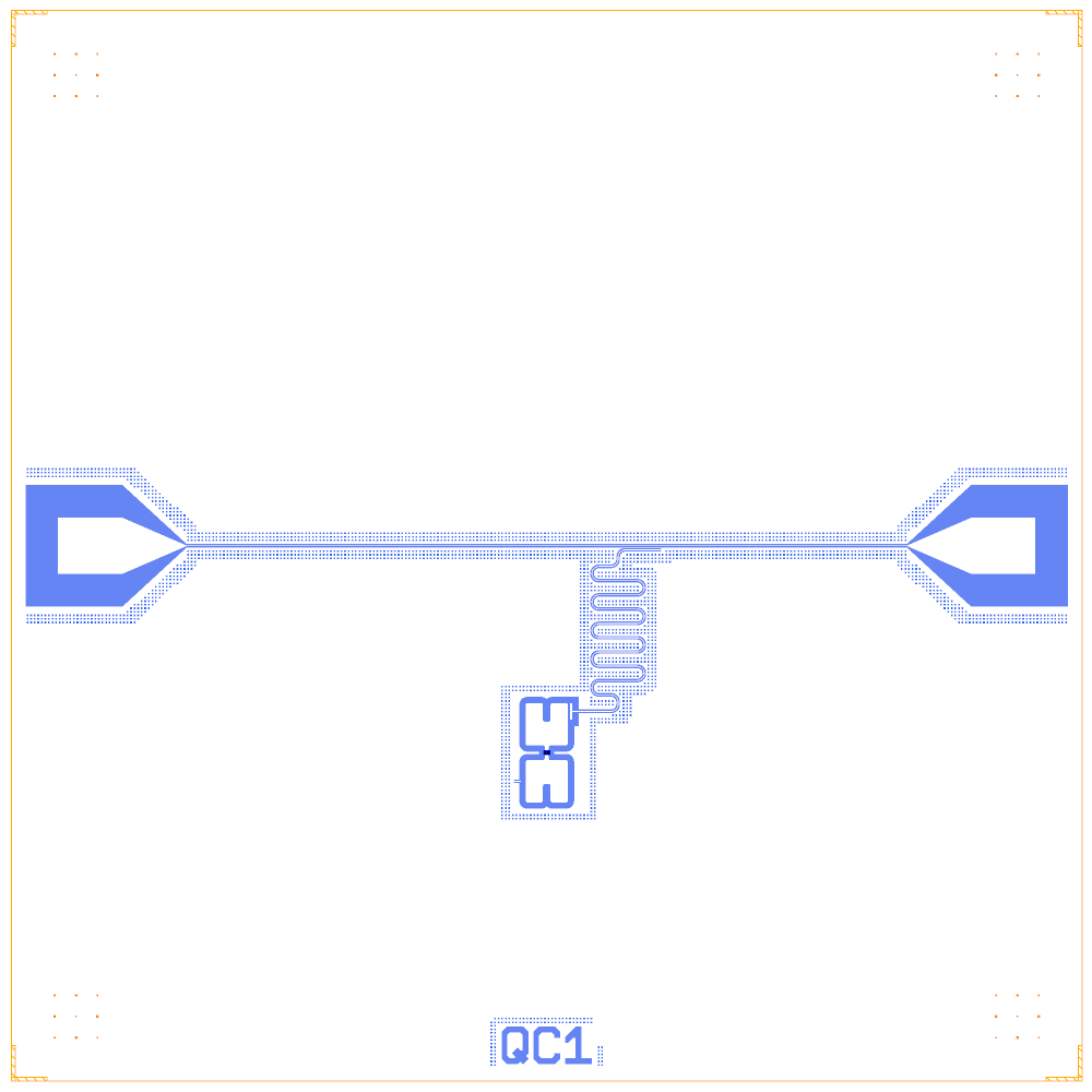
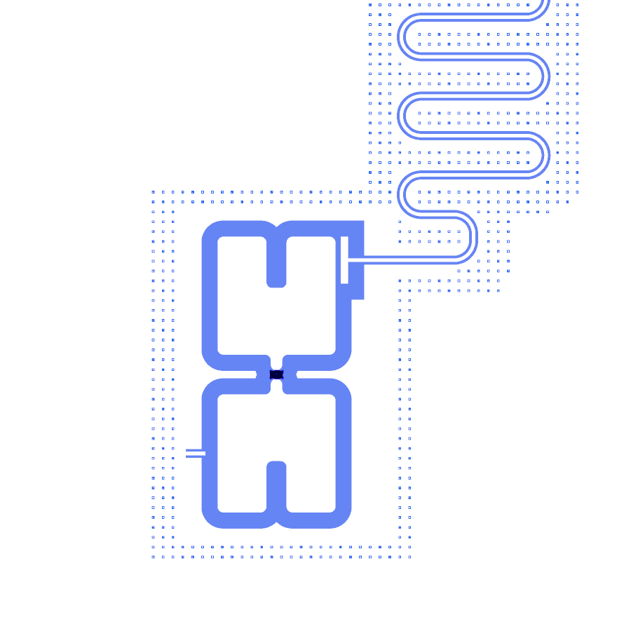
The DRC finds no error. It lists three warnings: the drive pin is not connected (nothing is routed to it on this
chip), and squid_a / squid_b are not routed (they are the junction-end markers of the simulation export).
d.drc()
8 · What the LOM says
from quantcore_circuits.circuit.fill import fill
from quantcore_circuits.lom.simulate import simulate

lb = d.lom()                                      # the netlist built from the component's fragment
res = simulate(fill(lb.model, d.design), max_modes=2)    # QuCat normal modes + QuTiP dressed values
The netlist has five nodes (FL, Q1.island1, Q1.island2, Q1.claw, ground) and ten branches. The values of
custom_qubits.ipynb, after one rescale of the resonator length (R1 = 4355 µm):
Quantity |
LOM |
|---|---|
C to ground, each island |
160 fF |
C between the islands |
12 fF |
C_g, island 2 to claw |
6.6 fF |
Junction |
L_J 7.01 nH, C_J 14.4 fF |
f_q |
5.595 GHz (target 5.5) |
α |
-193 MHz |
f_r |
6.992 GHz (target 7.0) |
χ |
-0.61 MHz |
κ |
0.21 MHz |
These are lumped-model estimates (rough formulas for a shape with no calibration), not FEM results; see
the LOM page for how far to trust them. The next step for a real design is a Q3D C-matrix of the cell
(q3d_cmatrix, nets Q1.island1, Q1.island2, Q1.claw): it replaces the three formulas by FEM values, and the LOM
runs again unchanged.
Next
From a drawn shape: the spiralmon builds a qubit from polygons instead of parameters.